Lab 4 - JFET Circuits I
University of California at Berkeley
Donald A. Glaser Physics 111A
Instrumentation Laboratory
Lab 4
JFET Circuits I
© 2016 by the Regents of the University of California. All rights reserved.
Microelectronic Circuits, Sedra & Smith Chapter 5
Microelectronic Circuits 5th Solutions Manual Sedra & Smith
Art of Electronics Student Manual, Hayes & Horowitz Chapter 3
The Art of Electronics, Horowitz & Hill Chapter 3
JFET Reading this is a big file so download it.
Curve Tracer Information at bottom of page
Physics 111-Lab Library Reference Site
Reprints and other information can be found on the Physics 111 Library Site.
NOTE: You can check out and keep the portable breadboards, VB-106 or VB-108, from the 111-Lab for yourself ( Only one each please)
In this lab you will explore basic JFET characteristics, circuits and applications. You will build a JFET switch, memory cell, current source, and source follower. Remember to keep your parts, do not lose them and do not return them to the parts cabinet.
Before coming to class complete this list of tasks:
- Completely read the Lab Write-up
- Answer the pre-lab questions utilizing the references and the write-up
- Perform any circuit calculations use MatLab or anything that can be done outside of lab use RStudio (freeware)
- Plan out how to perform Lab tasks.
- All parts spec sheets are located on the Physics Library site.
Pre-lab
1. What is the maximum allowed gate current? What happens if this current is exceeded?
2. In a few sentences, explain how a self-biased current source works.
3. Explain how to use load line analysis as outlined in the background materials. Why does it give the equilibrium current for the self-biased current source?
4. Why does increasing a follower’s source resistor ($R_S$) decrease its JFET’s transconductance? (Refer to the discussion in 4.16.) Why does this degrade the performance of a source follower?
Do not forward bias the JFET gates. Forward gate currents larger than 50mA will burn out the JFETs!
Background
JFET Transistors
There are two principle types of transistors: bipolar transistors (BJTs), and field-effect transistors (FETs). The physical mechanisms underlying the operation of these two types of transistors are quite different. We will limit our study to FETs because their physical mechanism is simpler. FETs are subdivided into two major classes: junction field-effect transistors (JFETs) and metal-oxide-semiconductor field-effect transistors (MOSFETs). (To be complete, each type of FET is further subdivided into n and p-channel FETs, and, for MOSFETs, enhancement and depletion MOSFETs, but we won't cover this now.)
Static electricity easily destroys MOSFETs; they can be burnt out simply by walking across a room on a dry day while carrying them in your hand. Once soldered into a circuit, however, MOSFETs are quite robust. Although MOSFETs are much more common than JFETs, we will work with JFETs because MOSFETs burn out so easily. JFETs will give us a good picture of how transistor circuits work.
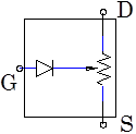
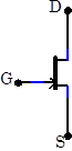
 Transistors are amplifiers; a small signal is used to control a larger signal. Typical transistors have three leads; in the case of a JFET, a voltage on one lead (called the gate) is used to control a current between two other leads (called the source and the drain). Of course, the gate voltage needs to be referenced to some other potential. By convention, it is referenced to the source. JFETs are drawn as shown to the right where the gate, drain and source (G, D, S, respectively) labels are normally omitted. Transistor voltages and currents are labeled by subscripts referring to the appropriate lead. Thus, $V_{GS}$ refers to the voltage between the gate and the source, $V_{DS}$ is the voltage between the drain and the source, $I_D$ is the current into the drain, and $I_S$ is the current out of the source. Under normal operating conditions, no current flows into the gate. Consequently $I_S=I_D$.
JFET Characteristics and the Transconductance Model
|
The JFET gate and drain-source form a pn junction diode; a very simple model of the JFET is shown at right. In this model the source to drain resistance depends on the gate bias. Under normal operating conditions, the JFET gate is always negatively biased relative to the source, i.e. $V_{GS}<0$. Consequently, the diode is reverse biased, and the gate current is negligible, thereby proving that $I_S=I_D$. The JFET may burn out if the gate is positively biased. This simple picture is the origin of the names for the leads. Electrons enters the device through the Source, exit through the Drain, and are controlled by the Gate. But by convention, we always speak of positive current flow; thus, though electrons enter through the Source and go to the Drain, positive current flows from the Drain to the Source. Checking the internal diode between the the gate and the drain-source with a DMM is a good, quick way of determining if a JFET is working; the diode is usually blown out in burnt out JFETs. |
Figure 1: Simple JFET Model |
|
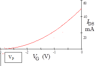
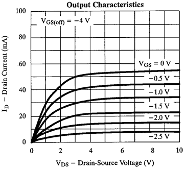
A more useful JFET model replaces the variable resistor with a variable current source whose current depends on the gate voltage $V_{GS}$ and the drain-source voltage, $V_{DS}$, as shown in Fig. 2. The drain-source current is largest when the gate-source voltage $V_{GS}$ is zero, typically about $50\,\mathrm{mA}$. As $V_{GS}$ is made negative, the current decreases. When the gate-source voltage $V_{GS}$ reaches a critical value called the gate-source pinch-off voltage $V_P$, the drain current $I_D$ is cutoff entirely; no current flows. (The pinch-off voltage is sometimes called the cutoff voltage.) The value of $V_P$ depends on the particular type of JFET (and even varies substantially between JFETs of the same type), but is typically around $-4$ to$-10\,\mathrm{V}$ . Thus, as $V_{GS}$ is raised towards $0\,\mathrm{V}$ from the pinch-off voltage, current $I_D$ starts to flow. A typical plot of the current vs. gate voltage is shown in Fig. 3 below left. Simple models of JFET performance predict that the curve will be parabolic, particularly near the pinch-off voltage, but actual devices may differ substantially from this prediction. The current $I_D$ will also depend on $V_{DS}$ as shown in Fig. 4 below right. Two regimes are apparent in the figure: a low voltage “linear” regime where the output current is linearly related to $V_{DS}$, and a “saturation” region where the current is almost independent on $V_{DS}$. JFETs are usually, but not always used in the saturation region, and the next two models model this regime only. |
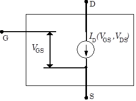 Figure 2: Transconductance JFET Model |
|
Figure 3: JFET Gate Transfer Characteristic |
Figure 4: JFET Output Characteristic. |
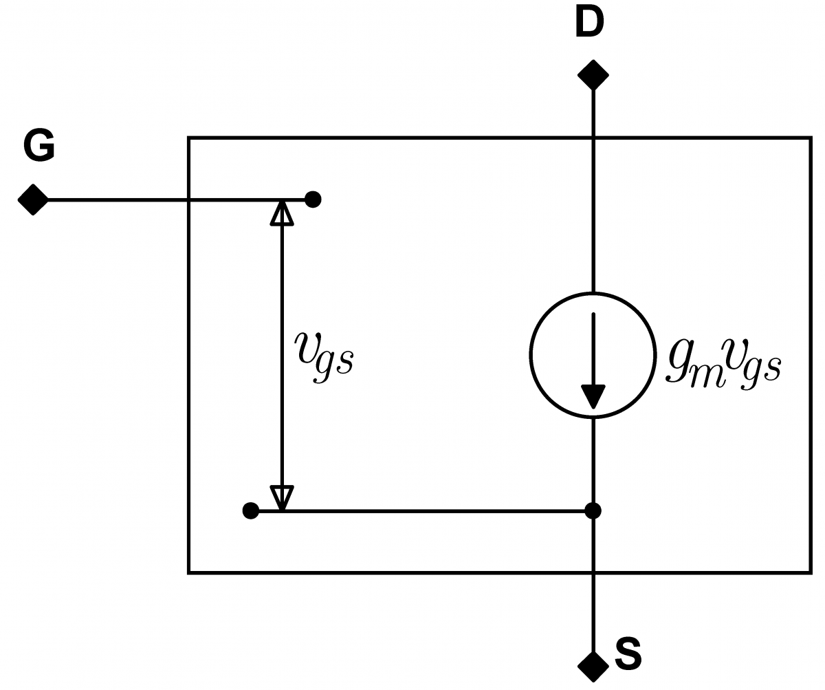
Small-Signal Transconductance Model
Circuits employing JFETs in the saturated regime typically keep the gate source voltage $V_{GS}$ relatively constant near some average value $\left<V_{GS}\right>$. In these circumstances, it is useful to consider a model for the JFET that is linearized around small variations $v_{gs}$ near $\left<V_{GS}\right>$, i.e. $v_{gs}=V_{GS}-\left<V_{GS}\right>$. By convention, the term of art “large signals” refers to the full, total voltage being applied, while the term of art “small signals” refers to small deviations from these large signals. We generally use capital letters for large signals quantities (like $V_{GS}$) and small letters for small signal quantities (like $v_{gs}$).
The simplest small signal model for the JFET is shown in Fig. 5 below left, and relates the linearized drain current $i_d=I_D-\left<I_D\right>$ to $v_{gs}$ through the linear relation $i_d=g_mv_{gs}$. The proportionality $g_m$ is called the “transconductance”; “trans” because the gate voltage is transferred to the source current, and “conductance” because $g_m$ has units of conductivity.
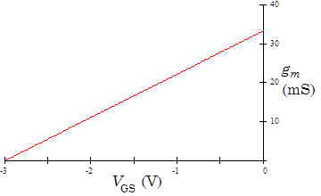
In any given circumstance, the transconductance is calculated by taking the derivative $g_m=dI_d/dV_{GS}$ at fixed $V_{DS}$. If the JFET transfer characteristic is a pure parabola like that shown if Fig. 3, then the transconductance will be a straight line like that shown in Fig. 6. The slope of the line will depend on $V_{DS}$, thus, the particular value of the transconductance to use in $i_d=g_mv_{gs}$ depends on both $\left<V_{GS}\right>$ and $\left<V_{DS}\right>$.
|
Figure 5: Transconductance model |
Figure 6: Transcounductance |
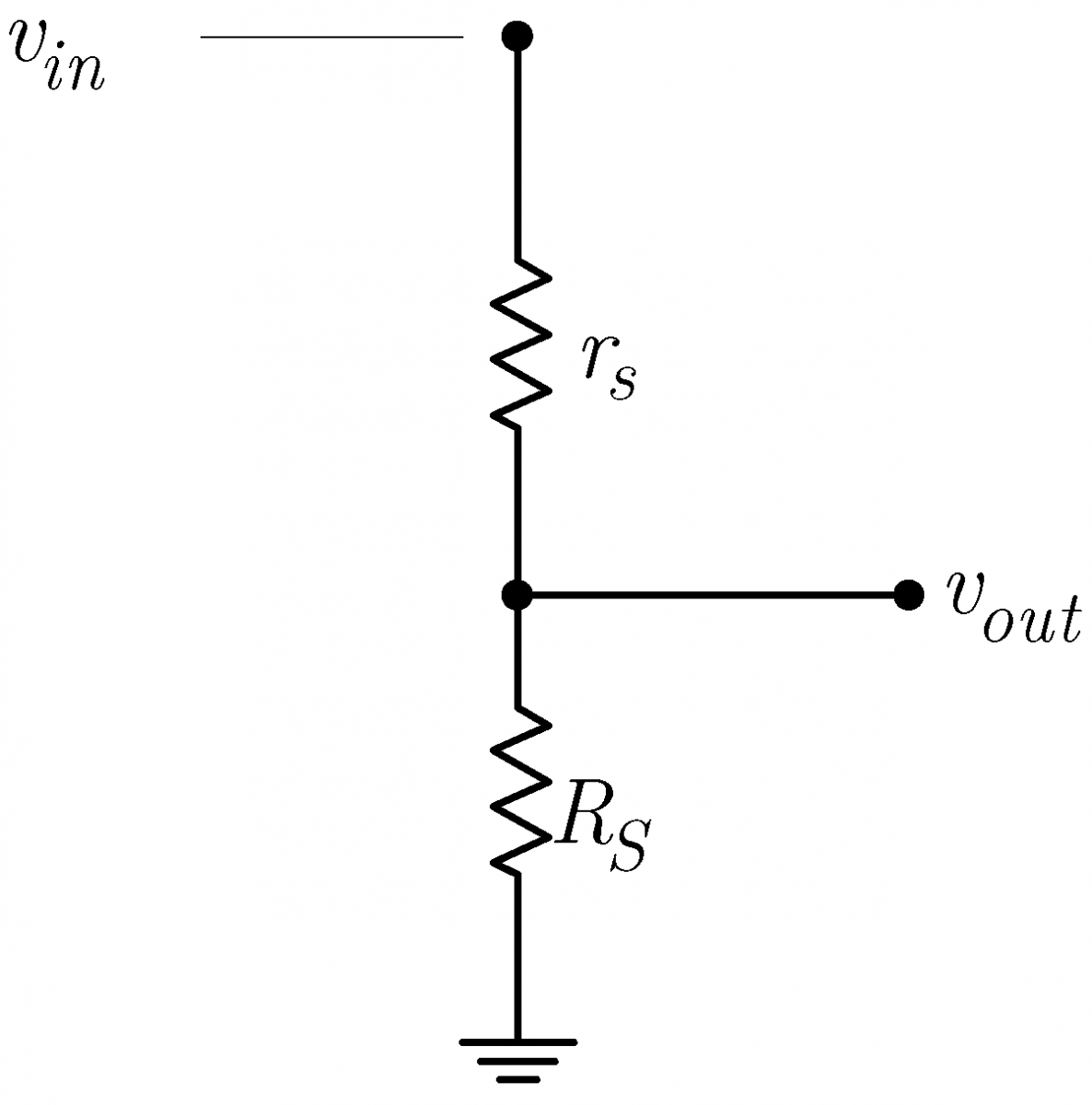
Small-Signal Source-Resistance Model
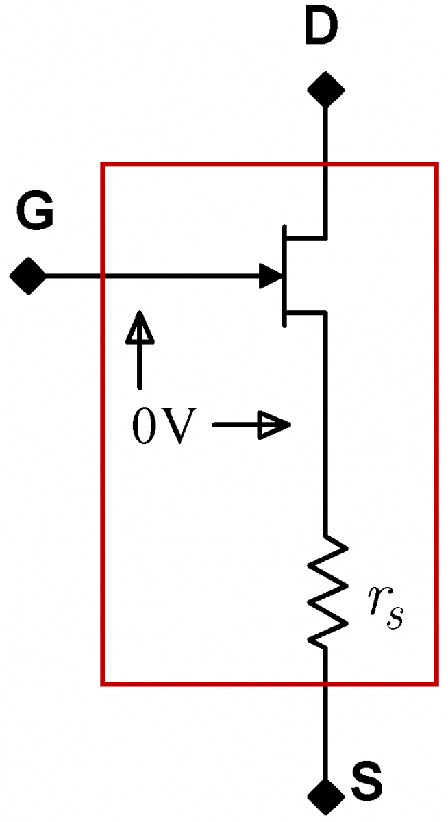
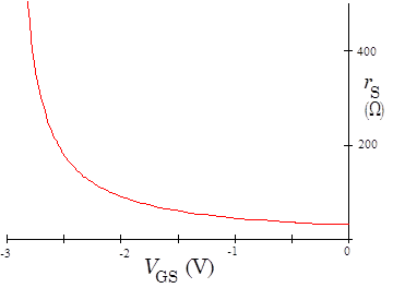
A useful variant of the transconductance model is the source-resistance model. This model consists of an ideal JFET connected to a source resistor, $r_s$ ,as shown in Fig. 7 below left. The value of the source resistor is $r_s=1/g_m$, and for a typical JFET, is graphed in Fig. 8 below right.
The ideal JFET passes whatever current is necessary to keep the gate and source at the same potential, hence the “$0\,\mathrm{V}$” in the model’s drawing. You can picture it as if there is a tiny Maxwell Demon that is constantly measuring the ideal JFET's gate source voltage, and adjusting the current through the JFET to keep this voltage at zero. Don't worry that this is a rather anthropomorphic picture, it is really quite useful.
We call the JFET in this model ideal because we pretend that its transconductance is infinite. Then, any desired current can be obtained with an infinitesimal $v_{gs}$, consequently $v_{gs}\approx0$. Ideal JFETs cannot be fabricated by themselves, in this model, the ideal JFET and the source resistor $r_s$ form an indivisible package. The ideal JFET’s source is internal to the package and is not accessible to the external circuit. As indicated by the label “S”, the “source” lead accessible to the external circuit is the lower end of the source resistor $r_s$. Don't worry that the internal ideal JFET has infinite transconductance, the complete device, including the source resistor, will not have infinite transconductance.
|
Figure 7: Source resistance model |
Figure 8: Source resistance |
Model Equivalence
The transconductance model and the source-resistance model are both small signal, i.e. linearized models. Though it may not be immediately obvious, they are formally equivalent. This equivalence is best established by an example.
- Consider a real JFET whose transconductance is $g_m=0.01\,\mathrm{S}$, and is driven by a voltage $v_{gs}=+0.1\,\mathrm{V}$. [The unit $\mathrm{S}$ is the unit of conductance, the siemens. You will sometimes see the archaic, but much more amusing unit, the mho (ohm backwards) for conductance.] Clearly, $i_d=g_mv_{gs}=0.01\times 0.1=0.001\,\mathrm{A}$ for the transconductance model.
- How does the ideal JFET in the source resistor model keep its gate and source at the same potential as is required in the source resistance model? It must drive enough current through the source resistor $r_s$ to raise the ideal source voltage (the voltage on the bottom lead of the inaccessible ideal JFET imagined to be inside the real JFET) to $+0.1\,\mathrm{V}$. Since the source resistance is $r_s=1/0.01=100\,\Omega$, this requires a current of $v_{gs}/r_s=0.1/100=0.001\,\mathrm{A}$.
Thus, both models predict the same current $i_d$. Since the models are equivalent, they will give the same results in any circuit. Personally, I (JF) find the source-resistance model easier to use.
To reiterate, all constant voltage offsets and constant currents are ignored in small signal models except in the initial calculation of the transconductance. In particular, the $V_{GS}$ bias required to obtain the desired $I_D$ is ignored; $v_{gs}$ is centered around zero. $V_{GS}$ is always negative; $v_{gs}$ can be positive or negative. The total current flow $I_D$ is always positive; $i_d$ can be positive or negative.
Self-Biased Current Sources
Current sources are very important in modern circuit design. A typical operational amplifier (op amp), a very common circuit that we will study extensively, might contain a dozen current sources. A JFET operated in the saturated regime functions as a current source; as you can see from Fig. 4, the Drain current $I_D$ rises only slowly when the Drain Source voltage $V_{DS}$ is increased. However, a JFET operating in isolation is not stiff enough ($I_D$ not sufficiently independent of $V_{DS}$) for most applications. Moreover, $I_D$ will vary substantially with temperature.
|
The self-biased current source depicted at right is a much stiffer source. As in any current source, the current through source, here down through the JFET $I_D$ , is almost independent of the voltage $+V$ across the circuit. (In an ideal, infinitely stiff source, the current would be entirely independent of $+V$.) The magnitude of the current can be programmed by changing the value of the resistor $R$. The behavior of this circuit is not obvious. The circuit depends on feedback: the output of the circuit controls its input. Feedback is an extraordinarily useful and general circuit design technique that has almost magical power. This self-biased current source is the first of many feedback circuits that we will study in this course. |
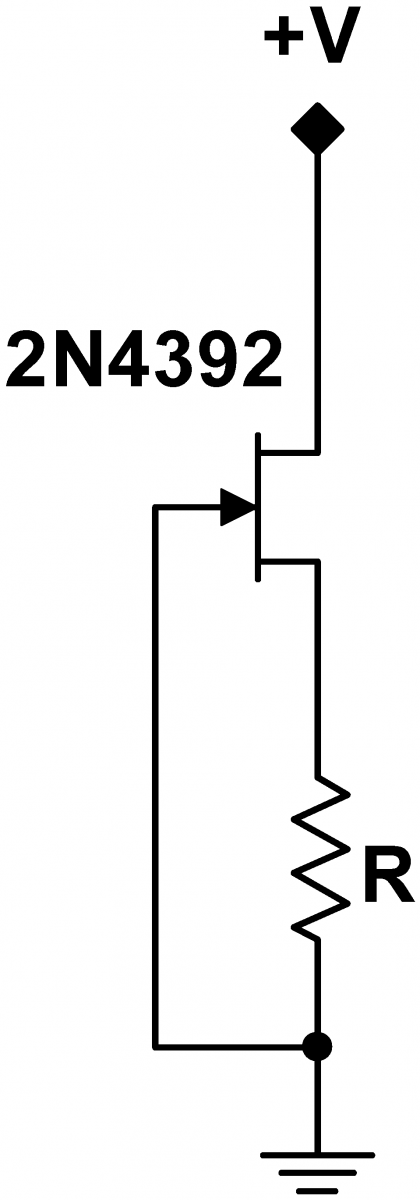 |
Let us consider how the above current source might startup when power is first applied. Imagine that the $+V$ source is turned on abruptly, and no current is yet flowing through the JFET. Then the voltage drop across the resistor will be zero, and the gate source voltage $V_{GS}$ will also be zero. But zero $V_{GS}$ allows large currents to flow through the JFET, so the current will increase. As the current increases, a voltage drop will develop across the resistor, and the upper end of the resistor will become positively biased relative to ground. This means that the gate will become negatively biased with regards to the source. Negative values of $V_{GS}$ will start to shut the JFET off. Eventually, a stable equilibrium will be attained where $V_{GS}$ is just right for the desired current to flow through the JFET.
Once in equilibrium, if the current were to increase, the voltage drop across the resistor would increase, the JFET source would become more positive, $V_{GS}$ would become more negative, and the JFET would shut off slightly. If the current were to decrease, the drop across the resistor would decrease, the JFET source would become less positive, $V_{GS}$ would become less negative, and the JFET would turn on slightly more.
In sum, the circuit regulates its output by feeding back a signal proportional to its output (in this case, the voltage across the resistor) into its input. In turn, this feedback to the input regulates the output.
|
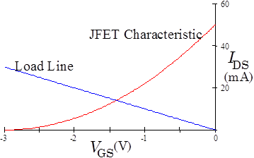
The equilibrium current through the JFET, i.e. the current source current, can be predicted by load line analysis. The graph at right plots the gate transfer characteristic in red. It also plots the load line $I_D=-V_{GS}/R$. Why does the load line graph have a negative slope? Think about the circuit carefully; for positive current running through $R$, the voltage across $R$ is the inverse of $V_{GS}$. Hence the negative sign. In analogy with the diode load line analysis, the JFET characteristic and the load line must be satisfied simultaneously. This will only occur at the two curve's intersection; this intersection, then, gives the equilibrium current. Why is this current source stiff? Consider variations in $+V$ and the corresponding variations in $V_{DS}$. These $V_{DS}$ variations will cause changes to the JFET characteristic curve, simplistically varying the coefficient of the parabolic dependence, and shifting the curve up an down. These variations will be small, however, if the JFET is in its saturated regime, where $I_D$ is relatively independent of $V_{DS}$. Then consider how the equilibrium point changes. If the load line has a small slope, the changes in the characteristic curve will primarily move the intersection point horizontally. The current $I_D$ will barely change. Consequently, the source will be stiff. |
 |
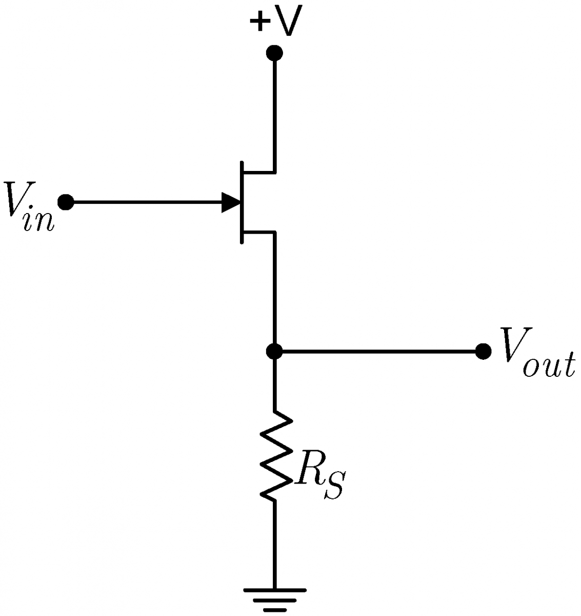
Source Followers
A follower is a circuit whose output voltage equals its input voltage. Since followers have no voltage gain, it might appear that they are useless. However, followers can have large current gains, which may be more important than voltage gain for high input impedance sources. For example, a common type of microphone has an output impedance near $1\,\mathrm{M}\Omega$, and puts out a signal of $10\,\mathrm{mV}$, leading to an output current of only $10\,\mathrm{nA}$. Such a tiny output current makes the signal difficult to use. If the signal were fed into a voltage follower with an output impedance of $100\,\Omega$ the current would increase to the much easier to work with value of $100\,\mu\mathrm{A}$, a current gain of $10^4$.
|
A particular type of follower, a source follower, can be constructed by slightly modifying a self-biased current source. Instead of grounding the gate as is done in the current source, the gate is driven by the input signal source as shown at right. The output is taken off the source resistor $R_S$. The notation is confusing here; this resistor, with a capital $R$, is a physical resistor attached to the JFET source. It is different from $r_s$ with a little $r$, the imaginary internal source resistor used in the small signal source resistance model. The circuit’s behavior changes little from that of the current source. Assume that with $V_{in}=0$ the current in circuit is $I_{D0}$. Then gate source voltage would be $V_{GS0}=-R_SI_{D0}$. If $V_{in}$ were to become positive, and $I_D$ did not change from $I_{D0}$, the gate source voltage $V_{GS}$ would increase, perhaps substantially. This would cause the JFET to want to increase $I_D$ which, in turn, would increase the voltage drop across $R_S$, thereby decreasing $V_{GS}$. We will see shortly that in equilibrium, the current $I_D$ would increase just enough that the gate source voltage would barely increase from its value of $V_{GS0}$. Similarly, if $V_{in}$ were to become negative, the equilibrium current would decrease just enough that the value of the gate source voltage would barely decrease from its value of $V_{GS0}$. Since $V_{GS}$ barely changes, the output voltage $V_{out}$ must track $V_{in}$, and the circuit acts like a follower. Note that track does not mean equal; thus, while the large signal $V_{out}\ne V_{in}$, the smal signal $v_{out}=v_{in}$. Remember that $V_{GS}$ always remains negative; the JFET gate is always reverse biased. |
 |
|
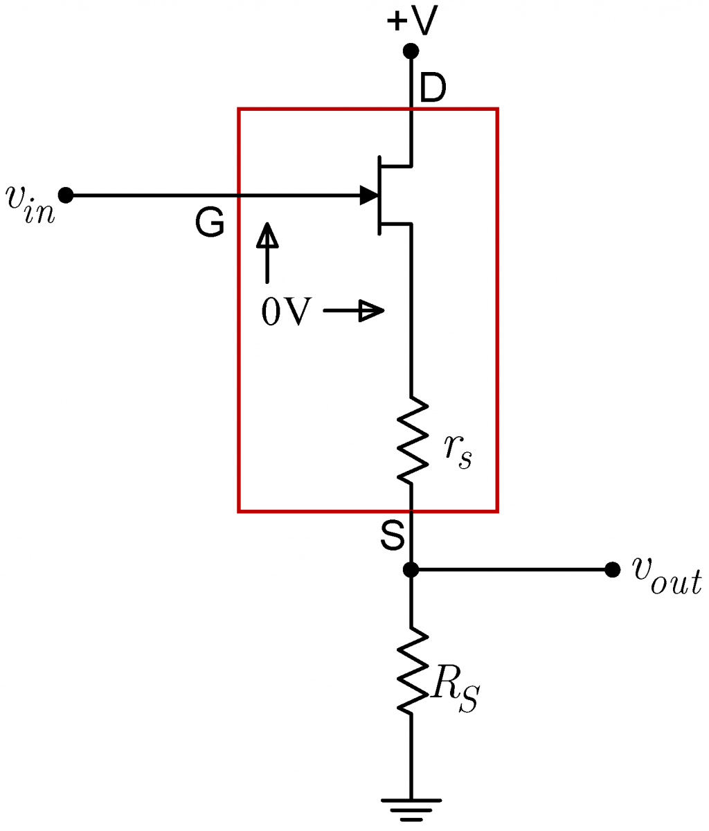
The follower’s small signal behavior can be described more accurately by replacing the JFET by its source-resistance model as shown at the immediate right. Remember that in this model, the ideal JFET keeps the internal source at the same potential as the gate. The model reduces to a voltage divider driven by a voltage-controlled voltage source as shown at the far right. Thus, the output of the circuit is $\displaystyle v_{out}=\frac{R_S}{r_s+R_S}v_{in}$. (1) So long as $r_s$ is much less than $R_S$, the output voltage will closely follow the input voltage. Using the model at the far right, we can easily calculate the output impedance of the follower. If we ground $v_{in}$ and look backwards into the circuit from $v_{out}$, we see the two resistors in parallel. Thus, the output impedance is $\displaystyle z_{out}=\frac{r_sR_S}{r_s+R_S}$. (2) So long as $r_s$ is small relative to $R_S$, the output impedance will be approximately $r_s$, and since $r_s$ itself is generally small, the follower's output impedance will be small. |
 |
 |
For further information about self biased followers, see Sedra & Smith, 2nd edition pages 282 through 287.
Packaging and Leads
|
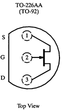
Transistors are manufactured in many different packages and sizes. Our 2N4392 JFETs come in a metal can. (Devices starting with 1N are always diodes; devices starting with 2N are always transistors.) As with many devices, the lead diagram depends on the view. A bottom view (immediate right) looks at the device from the lead side. A top view (center right) looks at the device from the non-leaded side. The 2N4392 leads are arranged in a triangle; the gate lead is the first lead clockwise from the tab when looked at in a top view. When inserting the JFET into the breadboard, there is no need to squash the leads out horizontally. In fact, doing so will risks accidentally shorting the JFET leads to the metal case. Instead of squashing the leads, just bend them out gently so that they form a triangular pattern, and are in different columns on the breadboard. It may be useful to have one of the leads span the breadboard's narrow socketless row region. |
Bottom View |
Top View |
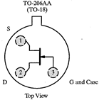 |
 2N4392
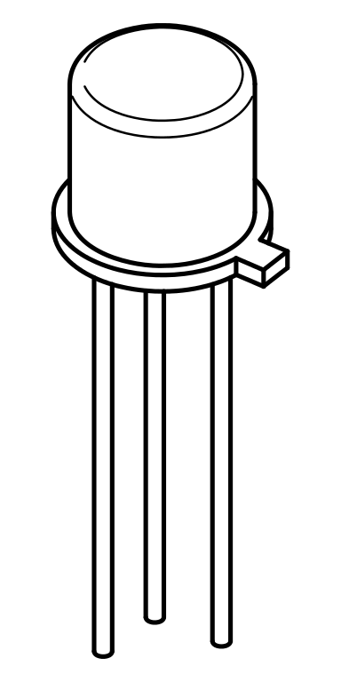
|
Many JFETs, including the 2N4392, are symmetrically constructed. The source and drain can be exchanged without changing the device behavior. But for simplicity, use should generally use the correct source and drain leads. Asymmetric JFETs, in which the source and drain cannot be exchanged, are normally drawn with an offset gate lead as shown at right. |
 |
In the lab
The properties of JFETs vary substantially from sample to sample. Unless otherwise noted, use the same JFET for all measurements measurements in this lab and in some of next week's lab. Make sure you keep your JFET separate. Build neat circuits with short wire lengths to minimize noise problems.
Problem 4.1 - Basic JFET Checks
Test that your JFET is working by doing DMM diode tests between the various pins. Describe the results of all your measurements.
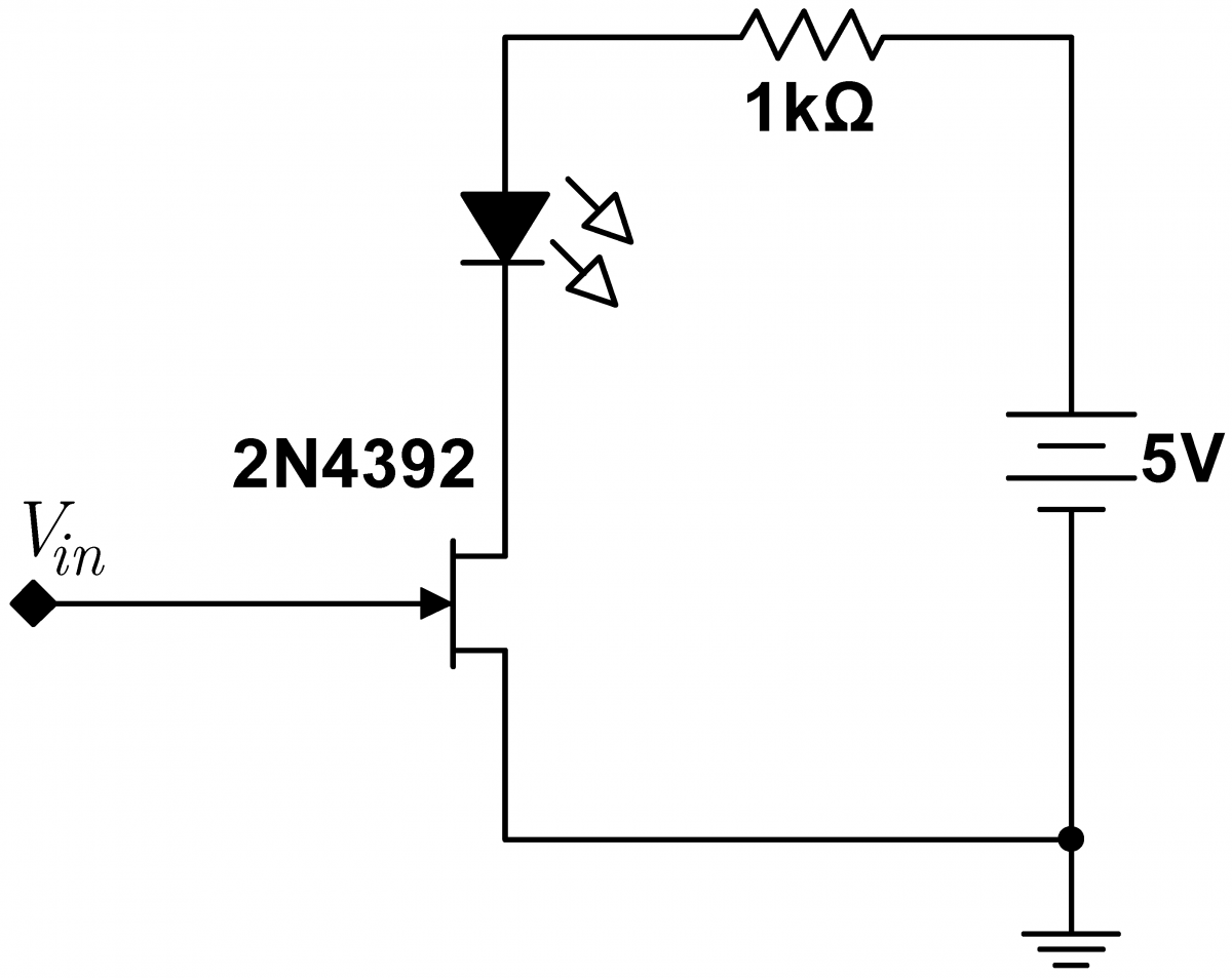
Problem 4.2 - JFET Switch
|
JFETs can be used as electronic switches. Build the circuit at right which switches an LED on and off. Touch the gate lead to ground to turn the LED on, and touch it to –12V to turn the LED off. So far, this switch is not very impressive; we could just as well have switched the LED on and off by moving its own lead rather than the JFET gate lead. Place a $22\,\mathrm{M}\Omega$ resistor in series with the gate lead. Can you still switch the LED? From 3.12, you know that the LED will not light when driven by a $22\,\mathrm{M}\Omega$ resistor. The JFET allows us to control the substantial LED current with the very small signal available through the $22\,\mathrm{M}\Omega$ resistor, thus demonstrating current amplification. |
 |
Problem 4.3 - JFET Memory
|
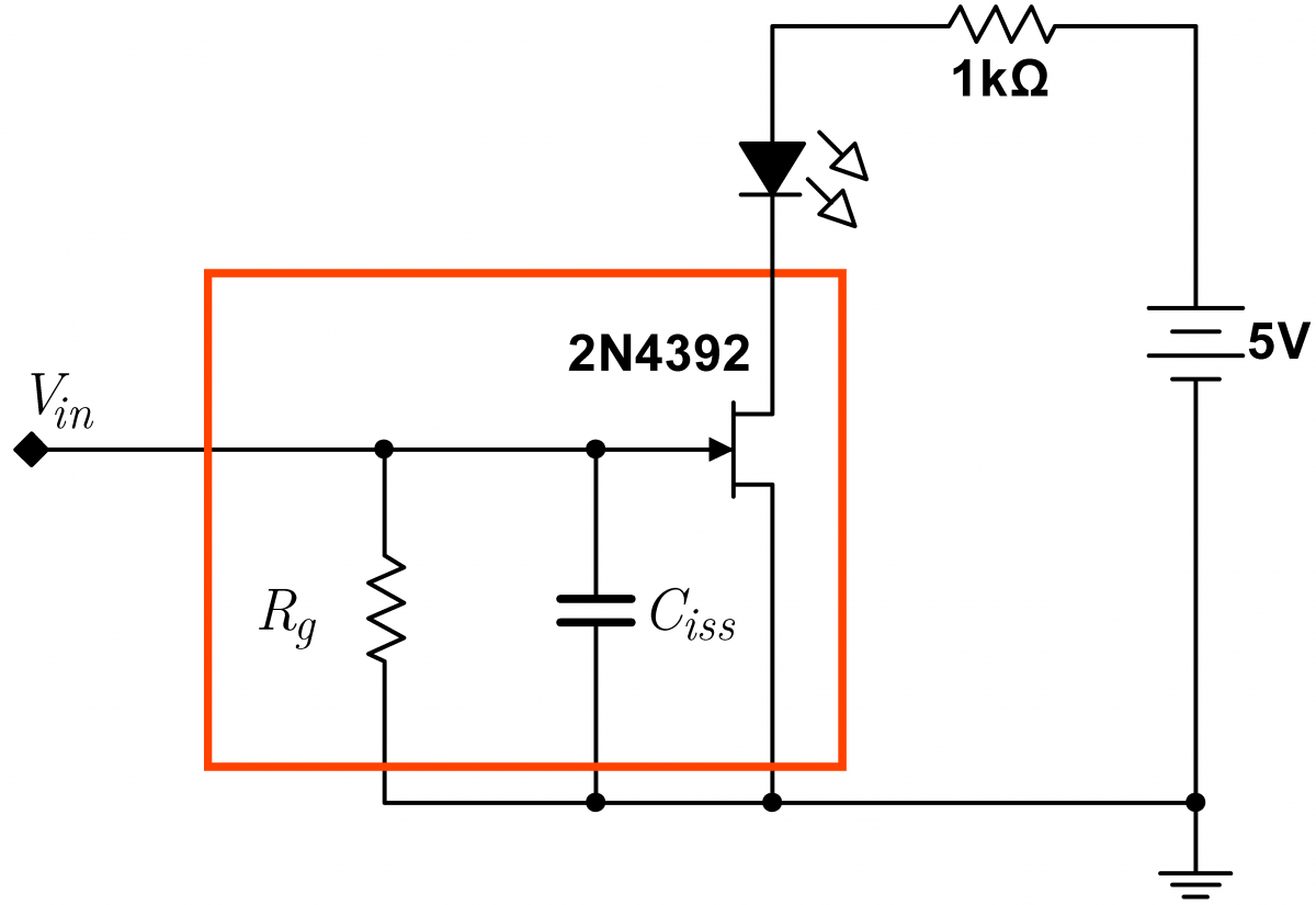
You may have noticed that the JFET switch remembers its last setting. Touch the gate to –12V for an instant and the LED stays off for a while; touch the gate to ground and the LED stays on. This memory results from the JFET’s intrinsic gate capacitance $C_{iss}$ and very high gate resistance $R_g$. $C_{iss}$is the capacitance that results from the finite physical dimensions of the JFET. This internal capacitance is not accessible from the outside of the device, and will vary from device to device. Likewise, the gate resistance $R_g$ is the resistance of the reverse biased gate diode, and is also not accessible from the outside and will vary from device to device. When the gate capacitor is discharged, $V_{GS}$ is zero and the JFET switch will be on. But when the capacitor is negatively charged, the JFET switch will stay off until the capacitor discharges, i.e. for a time on the order of $R_gC_{iss}$. The circuit can be redrawn with a JFET model (shown at right outlined in red) that includes these effects. |
 |
|
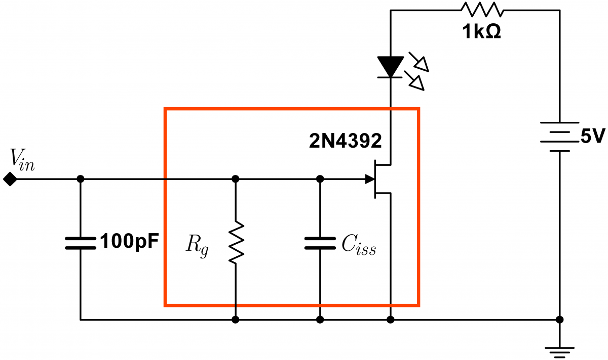
The memory time can be extended by adding an external capacitor. Measure the “forgetting” time with and without an external $100\,\mathrm{pF}$capacitor. Use a cell phone stop watch for timing. From these two times, determine the approximate values of $C_{iss}$ and $R_g$. Note that the resistance $R_g$ is very high. The memory time with the capacitor can be several minutes; if the time is impracticably long, use a $25\,\mathrm{pF}$ or $50\,\mathrm{pF}$ in place of the $100\,\mathrm{pF}$ capacitor. Note that tie capacitance and leakage resistance of the breadboard itself will influence your measured values by lowering the effective gate resistance and increasing the effetive gate capacitance. This memory effect is the basis for the dynamic RAM (Random Access Memory) found in computers., Computers use two types of memory. Static RAM (SRAM) remembers information forever, but is relatively expensive and cannot be packed tightly on a chip. Dynamic RAM (DRAM) is cheaper and smaller, and functions very much like the memory cell here. Virtually all the memory in a computer, often $4-16\,\mathrm{GB}$ (2016), is DRAM. The gate capacitance is very small for the FETs used in DRAM. The computer must remind, or refresh, the memory of its state every few milliseconds; first it has to read each memory bit to find out what state it is in, and then the computer refreshes the memory bit by the equivalent of touching the bit's gate to the appropriate potential. Hidden from the user, the computer must cycle through all of its memory this way every few milliseconds. |
 |
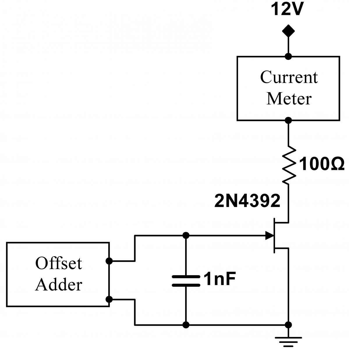
 Problem 4.4 - JFET Gate Transfer Characteristic
|
Build the circuit shown at right. Check your circuit before turning the power on; it is easy to burn out the JFET! Before you attach the offset adder to the JFET, make sure it is turned all the way negative to avoid JFET burnout. Use the scope or another DMM to measure the gate voltage. The $1\,\mathrm{nF}$ capacitor is in the circuit to suppress parasitic oscillations. Parasitic oscillations are high frequency oscillations that sometimes occur spontaneously. They are caused by unintended parasitic capacitances. These capacitances may be internal to the device, or result from the leads and wiring hooked up to the device. Lab 5 will discuss parasitic oscillations further. The $100\,\Omega$ limits the current so that the DMM fuse will not burn out. First find the most negative voltage for which drain current flows through the FET: the pinch-off voltage. Don’t be fooled by currents on the order of the lowest resolution measurable by the DMM. If the current does not depend on the gate voltage, these base-level readings are from the noise floor of the DMM. Find the gate voltage that just starts to increase the current. Then roughly determine the relationship between current and gate voltage by incrementing the gate voltage to zero, recording the current at approximately five points. |
 |
Problem 4.5 - JFET Gate Transfer Characteristic: Curve Tracer
Obtain the detailed transfer characteristic of your JFET with the computerized JFET Transfer Tracer option on the curve tracer. Plug your JFET into the Terminal Block provided with the curve tracer. You will find that the lead ordering on the JFET is reversed relative to the lead ordering on the Terminal Block. This would seem to require that the JFET leads be twisted. This is probably not a good thing to do; you will be using this JFET repeatedly in this lab, and you don't want to mangle the JFET leads. The tracer can be used without mangling the leads by using one or both of these solutions:
- The 2N4392 JFET is a symmetric JFET; the Source and Drain are technically interchangeable (though we do not generally advise you to do this). If you plug the JFET Source into the Terminal Block Drain, and vice versa, you will get the same characteristic curves as if you plugged the JFET in properly, even though the leads have been effectively reversed from the Tracer's perspective.
- If you swap the leads as in solution 1 immediately above, you can then rotate the Terminal Block by 180 degrees so that the Terminal Block Source is plugged into the Tracer Drain, and vice versa. From the Tracer's perspective, this will swap the leads yet again; this is one of those rare cases where two wrongs (two swaps) do make a right (no net swap).
Use the Tracer’s analysis option to fit the transfer characteristic to a parabola, and to find the transconductance $g_m$ and source resistance, $r_s$ as a function of $V_{GS}$. How close is the characteristic to a parabola? Is it at least a parabola over some limited range?
Plot all your data, and add the points that you took by hand to the transfer characteristic curve. For a gate voltage of $-1\,\mathrm{V}$, find the transconductance directly by differentiating the transfer characteristic curve, and check that your value agrees with the value automatically calculated by the Curve Tracer. The 2N4392 JFET is designed to be operated as a switch, and its transfer characteristic is far from ideal.
Finally, find the complete output characteristic for your JFET with the JFET Output Tracer option. Take scans in both the linear and saturated regimes.
Save this JFET for many of the remaining exercises.
Problem 4.6 - JFET Gate Transfer Characteristic: Curve Tracer for the 2N3819
|
Use the Curve Tracer to find the transfer characteristics of a 2N3819 JFET. Plot the transconductance of this JFET. The 2N3819 is a more typical and ideal JFET than the 2N4392; is its transfer characteristic closer to a parabola (that is, is its transconductance closer to linear)? Note that the 2N3819 uses the pin out shown at left. Specifications for the 2N3819 JFET are available on the course website. |
 |
Problem 4.7 - JFET Thermal Properties
Get a new JFET for this exercise only. You may have noticed in exercise 4.4 that higher drain currents $I_D$ drift downwards with time when $V_{GS}$ is held fixed . Investigate this effect: rebuild 4.4 with a new JFET, set the gate voltage for an $I_D$ of $1\,\mathrm{mA}$, and watch the current for a minute. Does it drift? Next, set the current to approximately $15\,\mathrm{mA}$. Now does it drift?
How much power is being dissipated by the JFET? Is the JFET hot? (Be careful, touch the JFET gingerly!) Obtain a can of Circuit Cooler. Spray the JFET for two seconds, and watch the current. How does it change?
Overheated components are a frequent cause of circuit failure. A common diagnostic technique is to spray a suspect component or circuit with circuit cooler, and see if the circuit begins to work again.
Note that Circuit Cooler works by releasing a pressurized gas, often 1,1,1,2-Tetrafluoroethane. The gas cools on expansion, and can be used to cool down your JFET. Formerly, we used Freon for the gas; Freon has some wonderful properties, but it destroys the ozone layer (contrary to assertions by Donald Trump). The gasses currently used are not so bad for the ozone layer, but do cause global warming. Too much use, and Holland and several Pacific Islands will be underwater in twenty years. Moreover, circuit cooler is expensive. Hence, minimize your use. Spray for only a second or two. Not much is required. Do not spray the cooler into your eyes or onto your body.
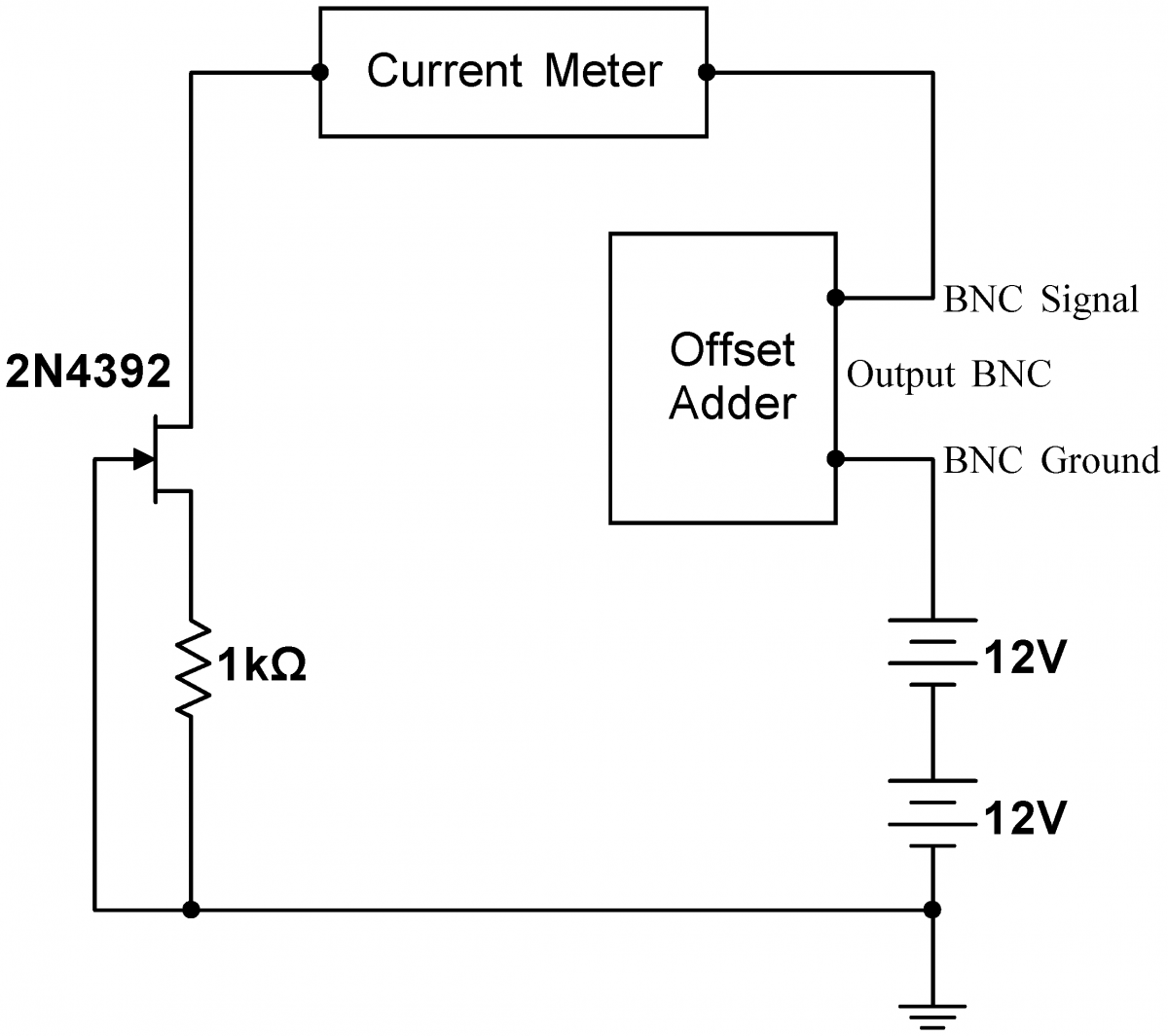
Problem 4.8 - JFET Self Biased Current Source
|
Build the circuit at right, with zero, one, or two of the $+12\,\mathrm{V}$ supplies in series with the offset adder output ground. Use the JFET whose characteristics you measured. Make sure that the base of the resistor and the JFET gate are connected to the hard ground associated with the $+5\,\mathrm{V}$ power supply. Note that offset adder input should float; nothing should be connected to it. In the diagram at right, the label "BNC Ground" indicates the outer conductor of the BNC output jack, which is NOT GROUNDED in this problem (The outer conductor of a BNC jack is often grounded, so it is called the "BNC Ground"). Adjust the Offset Adder to near zero to get a total voltage of $+15\,\mathrm{V}$ (within a few percent) across the JFET and resistor. (This is probably best accomplished using only one of the $+12\,\mathrm{V}$ supplies.) Measure the current going through the JFET. Adjust the value of the resistor until the current is between about $2.7\,\mathrm{mA}$ and $3.3\,\mathrm{mA}$. The closer you get to $3.0\,\mathrm{mA}$ the better, but you need not be obsessive. You may have to use multiple resistors in series or parallel. Measure and plot the current through the JFET $I_D$ as a function of the voltage across the JFET and resistor. Use combinations of the settings on the Offset Adder and zero, one, or two of the $+12\,\mathrm{V}$ supplies to explore positive potentials ranging from $+0\,\mathrm{V}$ to about $+35\,\mathrm{V}$. You should find that, past about $+3\,\mathrm{V}$ across the JFET and resistor, the current is nearly constant; this circuit is a good current source. Finally, set the Offset Adder and supplies back to yield a total voltage of $+15\,\mathrm{V}$. Briefly spray the JFET with circuit cooler. By how much does $I_D$ change? |
 |
Problem 4.9 - Adjustable Self Biased Current Source
For the circuit in 4.8, and with a total voltage of $+15\,\mathrm{V}$ across the JFET and resistor, measure and record the output current for the resistor you used in 4.8, and for resistor values of $100\,\Omega$, $390\,\Omega$, $3.3\,\mathrm{k}\Omega$, and $10\,\mathrm{k}\Omega$. Do the measured currents agree with the values predicted by a load line analysis based on the data from 4.5?
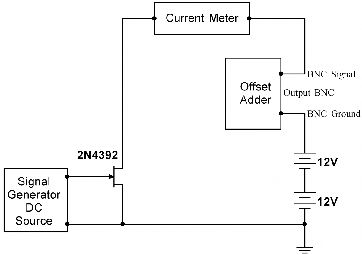
Problem 4.10 JFET Source-Drain Output Characteristics: Externally Biased Current Source
|
As discussed in the Background material, a self biased current source is better than a biased JFET current source. Prove this by building the biased JFET current source at right. It is quite similar to the circuit in 4.8; again, use zero, one, or two of the $+12\,\mathrm{V}$ supplies in series with the offset adder output ground. Make sure that the JFET source is connected to the hard ground associated with the $+5\,\mathrm{V}$ power supply. Use the Tektronix signal generator as a variable source of DC. (On the gnerator, use the front panel More Button -> More Screen Button -> DC to set the DC level.) Before energizing the JFET, set this level to $-3\,\mathrm{V}$ and check and see that $V_{GS}$ is indeed negative. Then energize your circuit, and adjust the DC level until you observe the same current as in 4.8 for $I_D$. Again, measure and plot the current through the JFET $I_D$ as a function of the voltage across the JFET and resistor. Use combinations of the settings on the Offset Adder and zero, one, or two of the $+12\,\mathrm{V}$ supplies to explore positive potentials ranging from $+0\,\mathrm{V}$ to about $+35\,\mathrm{V}$. The current should be approximately constant, but not as nearly constant as in 4.8. Finally, set the Offset Adder and supplies back to yield a total voltage of $+15\,\mathrm{V}$. Briefly spray the JFET with circuit cooler. By how much does $I_D$ change? |
 |
Problem 4.11 - Comparing Current Sources
Graph the current as a function of the voltage for exercises 4.8 and 4.10. Calculate the stiffness for both types of current sources: in an appropriate operating regime, find $\Delta I_D$ for some appropriately sized $\Delta V_{D}$. The stiffness is $\Delta V_D/\Delta I_D$.
You should have proved in 4.10 that the externally biased JFET current is approximately constant in the saturation regime. The operation of the externally baised source, which does not use feedback, is easier to understand than the operation of the self biased source. Why not use the externally biased current source circuit instead of the self-biased source of 4.8?
1. The self-biased source is stiffer. For fixed $V_{GS}$, the JFET current in 4.10 increases weakly with $V_D$. Hence the source is not perfectly stiff. But in the self-biased circuit, $V_D$ induced increases in the current will increase the voltage drop in the resistor, making the JFET gate more negative with regard to the JFET source, thus diminishing the current increase. While not perfect, the self-biased source will be much stiffer.
2. The self-biased source is much less temperature dependent. JFETs, like diodes, are strongly temperature dependent, but feedback acts to stabilize the current through the same mechanism described in the previous item.
3. The self-biased source has no external biasing network. The self-biased circuit is simpler than the external bias circuit because it does not need a negative bias power supply, and is thus completely independent of variations in such bias supply voltages. Consequently, the circuit can be powered by a wide range of supply voltages. Most op amps heavily rely on self-biased current sources, and will run on power supplies ranging from $\pm5\,\mathrm{V}$ to $\pm 18\,\mathrm{V}$.
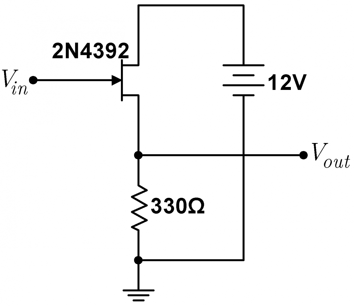
Problem 4.12 - Source Followers
|
Build the simple follower shown at right. Drive the follower with the waveform generator and Offset Adder. Play with different values of the offset, waveform amplitude, and waveform frequency, and compare $V_{out}$ to $V_{in}$. Notice that the output amplitude $V_{out}$ is slightly smaller than the input amplitude $V_{in}$ and also offset by a constant voltage. Can you explain the origin of the constant offset? |
 |
Problem 4.13 -Source Follower Gain
|
Remove the Offset Adder from 4.12, and drive the circuit with the signal generator directly. Carefully measure the follower's gain $G=v_{out}/v_{in}$. Because $v_{in}$ and $v_{out}$ are almost the same size, the gain can be determined most accurately by measuring the difference $\Delta v=v_{out}-v_{in}$ directly on the scope and calculating the gain from $G=1+\Delta v/v_{in}$. Note that here we are interested in the small signal components of the signals only: $v_{out}$, not $V_{out}$. The small signal components do not include any constant DC shifts; these shifts can be easily eliminated on your scope by using the AC setting. Determine the source resistance from the data of 4.5. Does the gain agree with the predicted gain from Eq. (1)? |
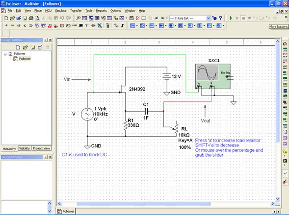
Problem 4.14
 |
Study the effect of a load resistor on a follower with the MultiSim Desktop\Mulitisim\Lab 4\Follower schematic, shown at right. The potentiometer default increment value (5%) is too big; set it to 0.1% be right clicking on the pot, going to the Value tab, and changing the Increment. Double click on the oscilloscope to bring up the scope graph, and run the simulation (by clicking on the green arrow run button or going to the Simulation menu and Selecting Run). Explore the effects of the load resistor by dragging the slider near the potentiometer or by pressing “a” and “Shift+a”. (Make sure the schematic is responsive to keys by clicking on it before trying the hot keys.) How does the output change? You will have to go to values below 10% to see a large effect. When the pot value equals the follower's output impedance, the output will fall by about a factor of two. Approximately what is the output impedance of the follower? From Eq. (2), predict the value of the internal source resistor $r_s$ and the transconductance $g_m$. |
 |
Problem 4.15 - Matching JFETs
Transistors with the same part number can vary significantly due to manufacturing variations. Consider, for example, the saturation drain current $I_{DSS}$, which is defined to be the current between the drain and the source when the gate source voltage is zero. For the 2N4392, this current is specified to be between $25\,\mathrm{mA}$ and $75\,\mathrm{mA}$; no typical or average value is given for this parameter.
Many circuits using multiple transistors work best if the transistors are nearly identical. Thus, it is important to develop techniques to select transistors that are nearly identical from a large stash; a set of nearly identical transistors is called a matched pair.
There are many parameters that could be matched, and there is no guarantee that matching one parameter, say $I_{DSS}$, will match other parameters, say $V_P$. Nonetheless, it is usually sufficient to match just one parameter, and assume that the other parameters will be close. On the surface, $I_{DSS}$ would be an attractive parameter to match, but in practice, it is not a good choice because of the large power dissipated in the FET when $V_{GS}=0$. Instead we will choose to measure the current $I_D$ of a current source with a fixed resistor.
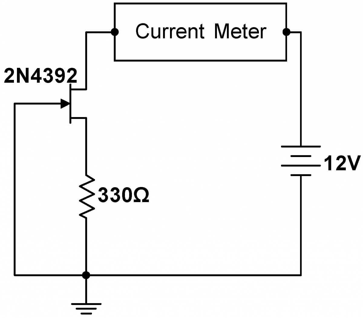
|
Build the current source at right. Obtain at least five additional 2N4392 JFETs and measure the current $I_D$ through each. Keep the JFET whose $I_D$ is as close as possible to the $I_D$ of your calibrated JFET (the one whose characteristic curves you measured). Your match should be within 10%. Return the other JFETs. Keep your matched pair for subsequent exercises in this Lab and in Lab 5. Note that the hand selection of matched pairs is not practical for commercial equipment. Fortunately it is rarely necessary because JFETs constructed on the same piece of silicon, such as in an integrated circuit, are very well matched. For the rare occasions when a discrete matched pair is required, very simple integrated circuits containing only a matched JFET pair are available.
|
 |
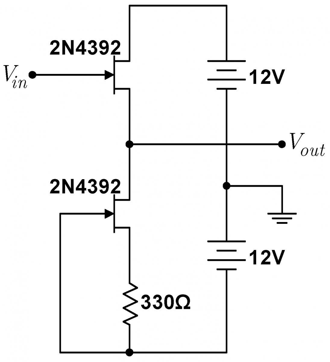
Problem 4.16 - Improved Follower I
The gain of the simple follower studied in 4.12‑4.13 is less than unity.
We need a way to effectively increase $R_S$ without changing $V_{GS}$. This can be accomplished by replacing $R_S$ with a current source. Since a current source is stiff, its effective $R_S$ can be very large, but since $I_D$ remains finite, it is clear from the JFET gate transfer characteristic (Fig. 3) that $V_{GS}$ remains in a region where the transconductance is large (Fig. 6).
|
Using your matched pair, construct the current-source driven follower diagrammed at right. Compare the input and output for a variety of input signals. Measure the gain. Is there any discernible difference between the input and output amplitudes? Using the stiffness of the current source calculated in 4.11 for $R_S$, the measured current $I_D$, and the internal source resistance $r_s$ found from combining the measured curves Fig 3 and Fig 8 for your JFET, calculate the gain. Does it agree with your observations?
|
 |
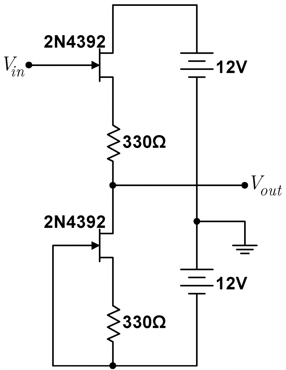
Problem 4.17 - Improved Follower II
|
The output of the follower in 4.16 is offset from the input by a constant voltage. Show that the offset will largely disappear if you insert a resistor as shown right. The gain will remain very near unity. Why does adding the second resistor get rid of the offset? Hint: Visualize the circuit with $V_{in}=V_{out}=0$. If this was literally true, how could you redraw the circuit diagram? Even with the second resistor, a small offset may remain. This remaining offset is likely due to imperfect matching of the JFETs, with a small contribution from imperfect matching of the resistors. |
 |
Analysis:
Problem 4.18 - Follower Feedback
JFET followers stay linear over a wide range of input voltages $V_{in}$, yet the gain depends on the transconductance $g_m$, which in turn depends on $V_{GS}$. Explain how feedback keeps the follower linear.
Please fill out the