Lab 6 - Op Amps I
University of California at Berkeley
Donald A. Glaser Physics 111A
Instrumentation Laboratory
Lab 6
Op Amps I
©2016 by the Regents of the University of California. All rights reserved.
Art of Electronics Student Manual, Hayes & Horowitz Chapter 4
The Art of Electronics, Horowitz & Hill Chapter 4
Physics 111-Lab Library Reference Site
Reprints and other information can be found on the Physics 111 Library Site.
In this week’s lab you will study op amps and feedback. You will construct a comparator, follower, current source, and inverting, non-inverting, differential, and summing amplifiers.
NOTE: You can check out and keep the portable breadboards, VB-106 or VB-108, from the 111-Lab for yourself ( Only one each please)
Before coming to class complete this list of tasks:
· Completely read the Lab Write-up
· Answer the pre-lab questions utilizing the references and the write-up
· Perform any circuit calculations use MatLab or anything that can be done outside of lab use RStudio (freeware).
· Plan out how to perform Lab tasks.
All Parts spec sheets are located on the Physics 111 Library site.
Pre-lab
1. Explain why the circuit in 6.2 exhibits hysteresis.
2. Design an inverting amplifier with a gain of ten and an input impedance of 1k.
3. What is the gain of the non-inverting amplifier used in 6.5?
4. Explain why the circuit below is a perfect current to voltage converter.
What is the conversion factor?
The Laboratory Staff will not help debug any circuit whose power supplies have not been properly decoupled!
Background
Integrated Circuit Amplifiers
As we have seen in the JFET labs, amplifiers constructed from discrete transistors have many undesirable features:
- High gain amplifiers are difficult to design.
- The amplifier’s gain is difficult to predict because it depends on the transistor’s transconductance, which varies between transistors.
- The gain depends on temperature.
- The amplifier’s output impedance is not low.
- Amplifiers made with bipolar transistors have low input impedances.
- Discrete transistors are easy to burn out. (This is a much bigger problem in our lab environment than in a production environment.)
Many of these problems can be eliminated by carefully designing complicated circuits using matching transistors. Such complete amplifier circuits, fabricated on a single piece of silicon, come prepackaged as “integrated” circuits (ICs). Many types of integrated amplifiers are available, but the most useful type is the Operation Amplifier (op amp).
Feedback
Op amps circuits almost always use negative feedback: feedback is the most important principle of modern analog circuit design. To apply feedback to an amplifier means to feed some of its output back into its input. There are two types of feedback:
- Positive feedback, where the output is used to enhance the input signal and increase the gain. Historically, positive feedback was (and is) used in oscillator circuits. Nowadays, positive feedback is also used in comparators and a few other circuits.
- Negative feedback, where the output is used to diminish the input signal and decrease the gain, seems foolish at first. After all, why deliberately diminish the gain of an amplifier? Indeed, negative feedback was greeted with incredulity when first invented by Harold Black and others in the 1920s. We shall see, however, that negative feedback dramatically improves the properties of amplifiers.
Op Amps
|
Op amps are high gain differential amplifiers. Like the discrete differential amplifiers that you built last week, op amps have two inputs $V_+$ and $V_-$, and one output, $V_\mathrm{out}$. Unlike discrete differential amplifiers, op amps have essentially infinite differential gain (gains over $10^7$ are readily available), negligible common mode gain, extremely high input impedance, very low output impedance, small temperature drifts and inconsequential piece-to-piece variation. Furthermore, they are insensitive to power supply fluctuations, are difficult to burn out, cheap, and available in countless varieties; one vendor, Digikey, sells over 30,000 varieties. Note that the op amp must also be connected to power; in our case to both $+12\,\mathrm{V}$ and $-12\,\mathrm{V}$. The power leads are typically not drawn. |
|
As op amps are almost always superior to discrete amplifiers, modern analog circuit designs use them almost exclusively. Real op amps are so close to being perfect amplifiers (i.e. infinite gain and input impedance, zero output impedance, etc.) that they are often thought of as being truly perfect. This pretense greatly simplifies circuit design. In this lab, we will generally assume that our op amps are truly perfect; the Op Amps III lab will investigate some of their limitations.
The Op Amp Golden Rules
1. The inputs draw no current.
2. The output attempts to do whatever is necessary to make the voltage difference between the two inputs zero.
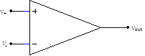
Op Amps Followers
|
The simplest op amp circuit is the follower. The first golden rule implies that the input impedance is infinite. The second rule is more interesting; since $V_-$ is wired to $V_\mathrm{out}$ , these two voltages must be equal. Likewise, $V_+=V_\mathrm{in}$. The only way that the two inputs can be at the same voltage, $V_+=V_-$, is for $V_\mathrm{out}=V_\mathrm{in}$. Consequently the op amp behaves like a perfect voltage follower. Understanding how the second rule is actually satisfied is particularly easy for the follower. If the output $V_\mathrm{out}$were to deviate low, $V_+-V_- = V_\mathrm{in}-V_\mathrm{out}>0$, the amplifier would drive its output $V_\mathrm{out}$ higher, reestablishing $V_\mathrm{out}=V_\mathrm{in}$. If the output $V_\mathrm{out}$ were to deviate high, $V_+-V_-<0$, and the amplifier would drive its output lower, once again reestablishing $V_\mathrm{out}=V_\mathrm{in}$. If the input voltage $V_\mathrm{in}$ were to change, $V_\mathrm{out}=V_\mathrm{in}$ would be similarly reestablished. Looked at in a bit more detail, one might be bothered by a seeming inconsistency. Since $V_+-V_- = V_\mathrm{in}-V_\mathrm{out}=0$ in equilibrium, and the output $V_\mathrm{out}$ is proportional to $V_+-V_- $, one might think that the output $V_\mathrm{out}$ must also be zero, not the desired $V_\mathrm{in}$. But remember that an ideal op amp’s gain is infinite. Since zero times infinity is undefined, it is not contradictory to set $V_+-V_- =0$ and $V_\mathrm{out}\ne0$. More realistically, the op amp’s finite gain means that the error voltage $V_+-V_- $ must be infinitesimally positive for $V_\mathrm{in}>0$, and $V_\mathrm{out}$ will settle to some value infinitesimally less than $V_\mathrm{in}$. Likewise, $V_\mathrm{out}$ will be infinitesimally greater than $V_\mathrm{in}$ for $V_\mathrm{in}<0$. Most precisely, $V_+-V_-=V_\mathrm{out}/G$, and $V_\mathrm{out}=V_\mathrm{in}/(1+1/G)$ for an op amp with gain $G$. Since $G$ is enormous for most op amps, the follower is essentially perfect. |
|
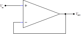
Op Amp Inverting Amplifiers
|
Another simple op amp circuit is the inverting amplifier. Here the inverting input $V_+$ is tied to ground. Since the second golden rule insists that $V_+-V_- $, the negative input $V_-$must also be at ground. As this ground is enforced by the op amp itself rather than by any physical connection to ground, it is often called a virtual ground. The current flowing towards the $V_-$ junction is then easy to calculate: $I=V_\mathrm{in}/R_1$. Since the first golden rule asserts that no current flows into the input itself, all of this current $I$ must flow out through the resistor $R_2$. Remembering that the $V_-$ end of $R_2$ is at virtual ground, the output of the op amp must be at $V_\mathrm{out}=-R_2I=-(R_2/R_1)V_\mathrm{in}$. Thus, the gain of the circuit is $-R_2/R_1$. |
|
Golden Rule Limitations
The golden rules apply only to circuits which satisfy the following requirements:
- The circuit must use negative feedback.
- There must be feedback at DC.
- The feedback must not push the output into saturation. (The golden rules must not demand that the output voltage be greater than the power supply voltages.)
Several circuits in this and the following labs will illustrate these limitations.
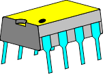
Packaging and Schematic Conventions
|
By convention, a DIP is always oriented so that the cut out is to the left (or up, if the dip is rotated by 90°.) Many of you will be tempted to ignore this convention, and you will get away with it for circuits that have only one or two op amps. But by the time you build circuits with ten op amps, as you will in later labs, randomly orienting the op amps will lead you to much confusion; better to get in the habit of orienting them properly from the beginning. Furthermore, orienting the circuits properly will make it much easier and faster for the GSI's to help you with debugging. |
 |
 |
|
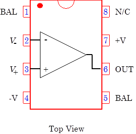
The pins on most op amps are connected as shown to the right. N/C stands for no connection, and should be left floating. The BAL pins are used to eliminate output voltage offsets caused by improper matching of the input transistors. These pins will not be used in this lab, and should also be left floating. The op amp power leads $+V$ and $-V$ must be connected for the op amp to work. Remember that the power leads are not normally drawn on circuit schematics. They must be connected to the +12 and -12 volt power supplies! Op amp circuits love to undergo parasitic oscillations. Always use power supply decoupling capacitors placed close to the op amps. $0.1\,\mu\mathrm{F}$ caps are a good choice. |
|
Comparators and Hysteresis
A comparator is a circuit that compares two voltages. An op amp used without feedback can function as a comparator. When $V_+-V_-<0$, the output will become as negative as it can, typically within a few volts of its negative power supply. When $V_+-V_->0$, the output will become as positive as it can, typically within a few volts of its positive power supply. These two conditions are sometimes called the low, or off state and the high, or on state, respectively.
Comparators are used in control circuits. A simple example is found in nighttime sensing street lamps. The lamps use a comparator to compare a signal from a light-sensitive photo detector with a reference signal. At nightfall the photo signal falls below the reference signal, and the comparator turns the street lamp on. At daybreak the photo signal rises and the comparator turns the lamp off.
Modern thermostatic-controlled house heating systems also use comparators to compare the output voltage from a temperature sensor to a reference voltage corresponding to the desired temperature. When the sensor voltage falls below the reference voltage, the comparator changes state, and turns on the furnace. As the furnace heats the house up, the sensor voltage rises, and the comparator eventually changes back to its original state, thereby turning the furnace off.
If a furnace was turned off the instant it raised a house’s temperature to the set point, and back on after the temperature fell just a bit, the furnace would cycle on and off frequently. Furnaces are inefficient when operated for very short periods of time. To avoid such cycles, thermostats are designed to turn off at a higher temperature than the temperature at which they turn on. For example the thermostat might be designed to turn on when the temperature falls below 66, and turn off once the temperature climbs above 68. Thus, when on, the furnace "overshoots" the desired set point, and won't turn back on until the temperature cools substantially.
This difference between the turn-on and turn-off temperatures is an example of a hysteretic effect. A hysteretic system is a system whose state depends on its history. Whether the furnace is on or off (its state) depends on both the temperature of the room and the history of the heating cycle (cooling down to the turn-on temperature, or heating up to the turn-off temperature.)
Street lamps provide an amusing example of the need for hysteresis. Inevitably, some of the lamp’s light couples back into its light detector, and this light might cause the lamp to turn off every time it turned on! Hysteresis prevents this sort of stuttering.
Op amps, used without feedback or with positive feedback, can be used as comparators, and we will use them this way in this lab. However, there are special purpose devices deliberately designed to be comparators, and they generally work better than op amps.
Photosensitive Devices
|
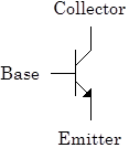
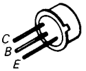
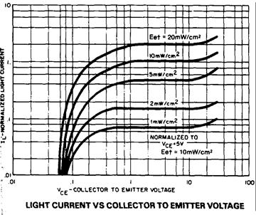
Semiconductor devices like photocells, photodiodes and phototransistors can react to illumination. Photocells sometimes called solar cells, convert light to electrical power, and are becoming increasingly cheap and practical. Photodiodes do not produce power, but are good light detectors. They are very similar to normal diodes, and are always operated reversed-biased. Remember that reverse-biased diodes do not conduct because of the absence of free carriers at their pn junctions; when a reversed biased photodiode is illuminated, photons create electron hole pairs in the junction region. The holes and electrons are swept in the appropriate direction by the junction’s electric field, causing a temporary, leakage-like current to flow through the junction. As the number of electron hole pairs created is proportional to the number of photons hitting the junction, and hence to the intensity of the light illuminating the junction, the total leakage current will be proportional to the light intensity. Any pn junction can show photo activity. Bizarre effects sometimes occur in our 1N4448 diodes because their glass packages allow light to strike the diode junctions. In this lab however, we will use a device optomized for light detection: the OP802SL bipolar phototransistor. Bipolar transistors come in two classes, NPN and PNP transistors, and are three leaded devices; the leads are called the collector, the base, and the emitter. The schematic for an NPN phototransistor is shown to the right. Our phototransistors come in a standard TO‑18 package, modified to include a plastic lens which focuses light onto the base junction. The emitter is the lead nearest the case tab, and the collector is the lead 180° from the emitter. The base is the lead in between. For a bipolar transitor, the collector is analogous to a JFET transistor’s drain, the base is analogous to a JFET’s gate, and the emitter is analogous to a JFET’s source. Bipolar transitor operation is roughly similar to JFET operation, but there are some very significant differences. The general use and operation of these transistors will be briefly discussed in the next lab. Despite our phototransistor being a three leaded device, we will leave the base unattached and connect only two of its leads, as if it were a photodiode. Even though it is not wired, the base increases the photransitor's light sensitivity compared to that of a simple photodiode. Shown to the right are typical curves showing the phototransistor output current between the collector and emitter, as a function of the collector to emitter voltage, for different illumination levels. Note that for collector to emitter voltages between 1 and 10V, the current is approximately independent of the collector emitter voltage; thus the phototransistor looks almost like a current source. |
  |
|
In the lab
Problem 6.1 - Comparators
|
Build the following comparator circuit, with $R_1$and $R_2 $ temporarily set to zero. For simplicity the V+ input is connected to the $+5\,\mathrm{V}$ supply, setting the comparator threshold at $+5\,\mathrm{V}$.More generally, the V+ input could be connected to any DC or AC signal. Show that the output switches between approximately $-12\,\mathrm{V}$ and $+12\,\mathrm{V}$ when the potentiometer voltage goes through $+5\,\mathrm{V}$. Look at the output on the scope. Can you adjust the potentiometer to obtain output voltages intermediate to $\pm12\,\mathrm{V}$? Why is this hard to do? Can you set a lower bound on the op amp gain? Now restrict the output range of the potentiometer to near $+5\,\mathrm{V}$ by setting $R_1=150\,\mathrm{k}$ and $R_2=100\,\mathrm{k.}$ Make sure that you can still get the output to jump between the two limits by turning the potentiometer.
By carefully tweaking the potentiometer, you should be able to get the output voltage to fluctuate between two values at one pot setting. These fluctuations are related to tiny fluctuations in the $+5\,\mathrm{V}$ power supply. If the output doesn't fluctuate, try adjusting the resistor values: $R_1=560\,\mathrm{k}$ $R_2=390\,\mathrm{k}$ may work, but these values may require tweaking if fully turning the pot doesn't cause the output voltage to switch. It may help to put a $0.1\,\mu\mathrm{F}$ across the LF356 power inputs (pins 4 and 7). Prove that the fluctuations are at $60\,\mathrm{Hz}$ by line-syncing the scope. Line sync is a trigger option, similar to aux and found on the same menu, that sync's the scope trigger to the $60\,\mathrm{Hz}$ oscillations of the $120\,\mathrm{V}$ power line. Noise and flucutations are often at this frequency, and, when examined on a scope set to line sync, will appear to partially freeze on the scope's display. Note that this circuit does not use feedback, and the golden rules do not apply. |
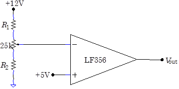 |
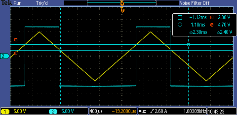
 Problem 6.2 - Hysteretic Comparator
|
The fluctuations that you observed in the previous problem can be eliminated by using positive feedback to provide hysteresis. Build the circuit at right, first with the $+5\,\mathrm{V}$ power supply. Show that the output cannot be made to fluctuate. Then disconnect the $+5\,\mathrm{V}$ supply from the Vin input, and connect instead a $500\,\mathrm{Hz}$, $20\,\mathrm{Vpp}$ triangle wave. Look at both the input and the output on the scope. You shold get traces that look like the image at right, showing the triangular input on channel 1 and the square wave output on channel 2. Look carefully at the input voltage at which the transitions in the output occur. You should observe that the output voltage switches high at an input voltage that is higher than the input voltage where the output switches low; this is the desired hysteretic effect. Determine the hysteresis (i.e. the difference between the turn-on and turn-off voltages.) It may be helpful to use the scope cursors. Note that this circuit uses positive feedback, and the golden rules do not apply; this is one of the very few times in this course that we will use positive feedback. |
 |
 |
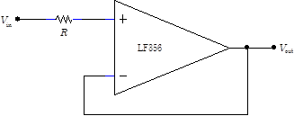
Problem 6.3 - Follower
|
Construct the follower like that show at right. Set $R=0$. By looking at $V_\mathrm{out}$, investigate the follower’s performance for a variety of input signals of different shapes, frequencies, and amplitudes. With a $1\,\mathrm{Vpp}$, $1\,\mathrm{kHz}$ sine wave input , vary $R$. Can you set a lower bound on the input impedance? Hint: Imagine that the op amp input looks like a voltage divider. Varying $R$ is like varying the top resistor in the divider. You may find that with sufficiently large resistors, say near $10\,\mathrm{M}\Omega$, you observe anomalies. Do these anomalies go away if you lower the frequency of your input signal to, say, $50\,\mathrm{Hz}$? |
 |
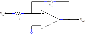
Problem 6.4 - Inverting Amplifier
Build the inverting amplifier that you designed in Pre-lab question 2. Carefully measure your circuits gain for a $0.2\,\mathrm{Vpp}$, $1\,\mathrm{kHz}$ sine wave. Does the gain agree with the design value? Now carefully measure the resistor values and calculate the expected gain. How does this gain compare with the observed gain?
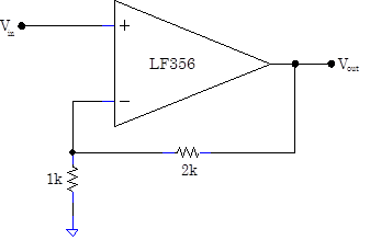
Problem 6.5 - Non-inverting Amplifier
|
Build the non-inverting amplifier shown at right, and measure its gain. How does its gain compare with the design gain calculated in Pre-lab question 3? Now carefully measure the resistor values and calculate the expected gain. How does this gain compare with the observed gain? |
 |
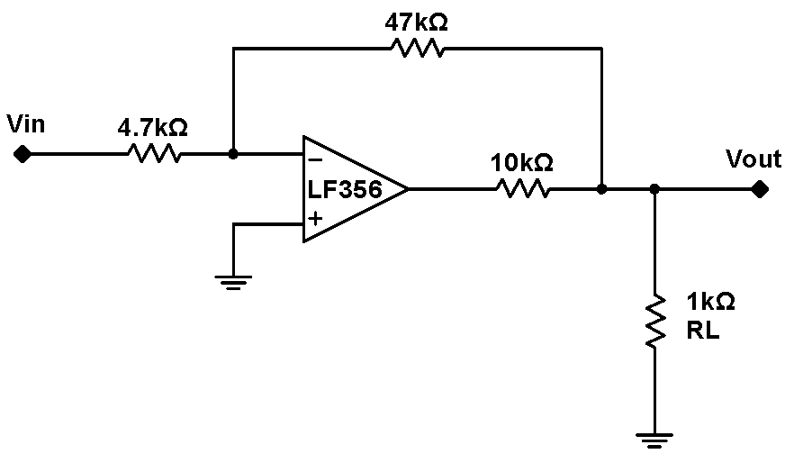
Problem 6.6 - The Virtues of Feedback
|
Build the inverting amplifier shown at right. This amplifier has an unusual, and under some circumstances deleterious, $10\,\mathrm{k}$ output resistor. This resistor degrades the normally very low op amp output impedance to $10\,\mathrm{k}$. This is a fairly high output impedance. Nonetheless, feedback will cure the deleterious effects of the high impedance in some circumstances. With the $1\,\mathrm{k}$ load resistor $R_\mathrm{L}$ temporarily removed, what is the gain of the circuit for a $0.1\,\mathrm{Vpp}$, $1\,\mathrm{kHz}$ sine wave? For a $1\,\mathrm{Vpp}$ sine wave? (Make sure that the signal generator output is set to High Z, and make sure that your smaller signal really is $0.1\,\mathrm{V}_\mathrm{pp}$.) Is the gain what you would expect for both cases? Now insert $R_\mathrm{L}$ and repeat. Does the amplifier still work for both input voltages? Is the gain the same with and without the load resistor at both input voltages? You might wish to also examine the response of the circuit with a triangular wave. What causes the circuit failure at $1\,\mathrm{Vpp}$ with the load resistor? Hint: Think about what the output voltage of the LF356 would have to be for this circuit to work with a $1\,\mathrm{Vpp}$ input. Feeback normally works beautifully, but it cannot fix fundamental component limitations. |
|
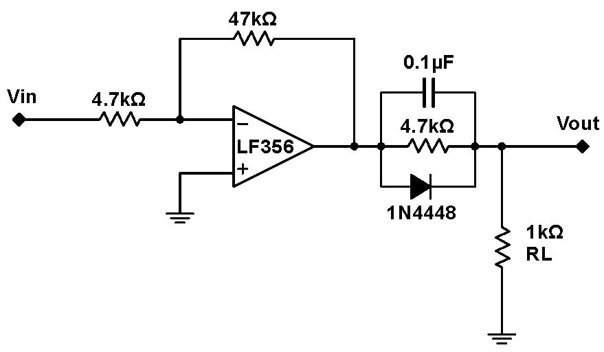
Problem 6.7 - Even More Virtues of Feedback - I
|
Drive the circuit at right with $0.1\,\mathrm{Vpp}$ and $1\,\mathrm{Vpp}$ sine waves. Record images of the output at $100\,\mathrm{Hz}$ and at $10\,\mathrm{kHz}$. You should observe that, under some circumstances, the diode-cap-resistor network greatly degrades the amplifier. Note that the feedback loop does not include these circuit elements. Explain the influence of the diode and the capacitor. |
|
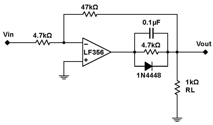
Problem 6.8 - Even More Virtues of Feedback - II
|
The circuit in 6.7 is frequency dependent and powerfully nonlinear. If the frequency dependent and nonlinear elements are included inside the feedback loop, the circuit will behave much better. Change the feedback point to the position shown at right. What is the output now with $0.1\,\mathrm{Vpp}$ and $1\,\mathrm{Vpp}$ inputs and at $100\,\mathrm{Hz}$ and $10\,\mathrm{kHz}$? Record typical images. Is the circuit frequency dependent? Is it nonlinear? You should observe that proper feedback can cleanup horribly nonlinear and frequency dependent behavior. Feedback will take a poor quality op amp, like the "composite" op amp investigated here (the LF356 and the diode, resistor and capacitor) and make it function well. |
|
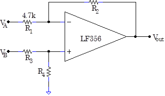
Problem 6.9 - Differential Amplifier
|
Finish the design of this gain-equals-ten differential amplifier. Construct the circuit. Does it work? Measure the common mode gain, and the gain on each input with the other input grounded. Do these gain agree with what you would predict? Measuring the gain of one input with the other input grounded isn't quite the same as measuring the differential gain. To make a true differential gain measurement, you need both your original input signal and its inverse. Use an inverting op amp follower to generate this inverted signal, and feed both the orignal and the inverse into your differential amp. Now measure the true differential gain. |
 |
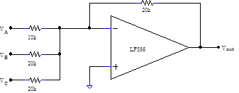
Problem 6.10 - Summing Amplifier
|
Op amps can be used to sum signals. Construct the circuit at right, and show that its output equals$-(2V_A+V_B+V_C)$. The Offset Adders which are part of your breadbboard box use a summing circuit similar to this with one input attached to a potentiometer. |
 |
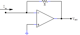
Problem 6.11 - Current to Voltage Converters
|
Use the circuit at right to transform the current signal from the OP802SL phototransistor into a voltage signal. How does the voltage signal change if you wave your hand over the phototransistor? Hook an LED up to the signal generator, and drive the LED with a 1kHz square wave. Place the LED next to the phototransistor. Can you pick up its modulated light signal? Prove that the circuit is detecting the light signal rather than some sort of electrical pickup signal by interposing a paper sheet between the LED and the phototransistor. The paper, unlike your hand, is nonconductive and will not act like an antenna and influence the circuit. |
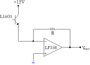 |
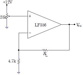
Problem 6.12 - Op Amp Current Source
|
Op amps can be used to make excellent voltage-controlled current sources. In the circuit at right, set the potentiometer output to about $+3\,\mathrm{V}$, and measure the current through a load resistor $R_\mathrm{L}$ of $4.7\,\mathrm{k}\Omega$with a multimeter. Swap in different load resistors while measuring the current. Find the range of $R_\mathrm{L}$ over which the current does not vary significantly. Restore the load resistor to $4.7\,\mathrm{k}$, and vary the potentiometer voltage. How does the current change? |
 |
Analysis
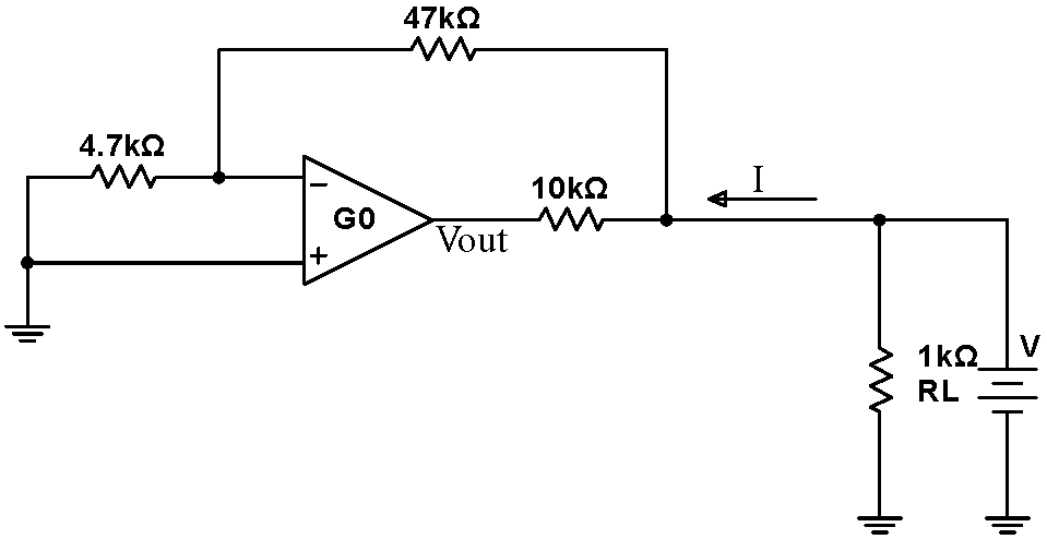
Problem 6.13 - Output Impedance Calculation
|
Assuming that the op amp has a finite gain $G_0$, but is otherwise ideal, what is the output impedance for the amplifier (the entire amplifier, including the $4.7\,\mathrm{k}\Omega$, $47\,\mathrm{k}\Omega$ and $10\,\mathrm{k}\Omega$ resistors) in 6.6? One way to determine the output impedance is illustrated at right. One imagines hanging a voltage source $V$ on the output, and measuring the current $I$. Then $Z_\mathrm{out}=V/I$. To calculate the current, one needs the open loop gain $G_0$ (usually called $A_0$ on spec sheets). This gain is typically very high, often in the millions near DC. Since the positive input terminal is grounded, $V_\mathrm{out}=-GV_-$. But $V_-$comes from input and feedback resistor voltage divider. Once $V_\mathrm{out}$ is known, the current $I$ is just the sum of the current into the feedback $(47\,\mathrm{k}\Omega)$ resistor and the current into the $10\,\mathrm{k}\Omega$ resistor. (Simplify your answer by taking advantage of the fact that $G_0$ is very large.) You should ignore the load resistance $R_\mathrm{L}$ throughout this calculation. Your should find that the output resistance is very low. So why does the op amp fail under certain conditions (large input drives) when the circuit is loaded? |
 |
Problem 6.14 - Summing Amplifier Calculation
Prove that the output of 6.10’s circuit is $-(2V_A+V_B+V_C)$.
Explain why 6.12 is a constant current source. What determines its output current? What limits the size of the load resistor?
After completing the lab write up but before turning the lab report in, please fill out the Student Evaluation of the Lab Report.