Lab 8 - Op Amps III
University of California at Berkeley
Donald A. Glaser Physics 111A
Instrumentation Laboratory
Lab 8
Op Amps III
© 2015 Copyright by the Regents of the University of California. All rights reserved.
Microelectronics Circuits, Sedra & Smith Chapter 2, skim Chapters 4, 9, & 10
Art of Electronics Student Manual, Hayes & Horowitz Chapter 4
The Art of Electronics, Horowitz & Hill Chapter 4, skim Chapters 2, 8.1
Physics 111-Lab Library Reference Site
Reprints and other information can be found on the Physics 111 Library Site.
NOTE: You can check out and keep the portable breadboards, VB-106 or VB-108, from the 111-Lab for yourself ( Only one each please)
In many circuits, op amps behave perfectly in the sense that the op amp golden rules are obeyed. However, some circuits expose op amp imperfections which violate the golden rules. This week’s lab explores some of these circuits, and investigates methods of curing some of the imperfections.
Before coming to class complete this list of tasks:
· Completely read the Lab Write-up
· Answer the pre-lab questions utilizing the references and the write-up
· Perform any circuit calculations use MatLab or anything that can be done outside of lab RStudio (freeware).
· Plan out how to perform Lab tasks.
All parts spec sheets are located on the Physics 111 Library site.
Prelab
1. Explain why it is necessary to divide by 1000 to obtain the input offset voltage Vos in 8.1.
2. Why does the capacitor in 8.3 mask 60Hz noise?
3. How does the push-pull circuit in 8.11 work? What do you think is the origin of the name?
The Laboratory Staff will not help debug any circuit whose power supplies have not been properly decoupled!
Background
The last two week’s exercises should have convinced you that op amps behave ideally in a wide range of useful circuits. However, in certain circuits, op amps have imperfections which break the golden rules. The most important imperfections can be divided into four categories:
I Input Imperfections
I.1 Voltage Offset
The transistors and other circuitry in an op amp's differential input stage do not match perfectly. Consequently, the op amp's output is not precisely zero when $V_+=V_-$. The input offset voltage, $V_\mathrm{os}$, is the input voltage differential $V_+-V_-$ that produces zero output voltage. The input offset voltage varies between devices. Typical and max values of $V_\mathrm{os}$ are given on spec sheets.
I.2 Input Bias Current
All op amp inputs sink or source current. The average of the currents sinked or sourced by the two inputs is called the input bias current $I_\mathrm{B}$. It is independent of any currents due to the op amp’s finite input resistance; the inputs attempt to sink or source current even when grounded. Potential drops induced by the input currents as they flow through the input and feedback resistors can introduce significant output errors. Like the offset voltage, the current bias varies between devices.
I.3 Input Offset Current
The difference between the current sinked or sourced by the two inputs is called the input offset current Ios. The offset current is typically one-half to one-tenth as large as the input bias current.
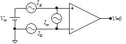
Figure 1 Voltage and current biases necessary to produce zero output voltage.
II Output Imperfections
II.1 Finite Output Voltage Swing
An op amp’s output voltage cannot exceed its power supply voltages; for many op amps, it must be a few volts less than the power supply voltage. The golden rules will be violated if the feedback network requires the output to swing beyond these limits. Examples of this limitation have appeared in the previous op amp labs.
II.2 Finite Current
The op amp output current is limited to some finite value, typically around ±20mA. Frequently, this limit is deliberately designed into the op amp circuitry to ensure that the output can be safely shorted; some op amps, however, are not protected and can be blown out by shorting their outputs.
III Noise
III.1 Voltage Noise
Ideally, an op amp’s output would be constant when its inputs are held at fixed values. Unfortunately, the output of all practical op amps fluctuates, and only averages to a fixed value. These fluctuations are called noise. Noise degrades circuit performance; high noise levels can overwhelm a circuit’s desired signal.
For many noise sources, the fluctuation amplitudes are gaussian distributed. Moreover, the noise has no dominant or characteristic frequency. All frequencies have the same noise power. This particular type of noise is called white noise.[1]
Op amps typically produce white noise. One op amp noise component[2] is the voltage noise, $e_n$. Voltage noise is specified in volts per root hertz. The op amp behaves like a noiseless op amp whose inputs are in series with a white noise source of rms amplitude $e_n \sqrt{B}$ , where $B$ is the bandwidth over which the output is examined. For example, a typical op amp might have a voltage noise of $10 \, nV/\sqrt{Hz}$. Used in a circuit with a bandwidth of $100\, Hz$ to $10\, kHz$ , the total noise would be $10^{-8} \sqrt{10000-100} \, V \approx 10^{-6} \, V = 1 \, \mu V \, (RMS)$ .
III.2 Johnson Noise
The resistors used in an op amp’s external circuit are also noisy. Resistor noise, also called Johnson, Nyquist, or thermal noise, results from the thermal fluctuations of the resistor’s electrons, and is proportional to the square root of the resistance, temperature and bandwidth.[3]
IV Frequency Dependent Imperfections
IV.1 Finite Gain
Although an ideal op amp has an open-loop (no feedback) gain of infinity, all practical op amps have finite open-loop gains, typically around $10^5$ at DC. So long as the closed-loop (with feedback) gain is substantially lower than the open-loop gain, say by $10^3$, the errors due to the finite gain will be unimportant. This criterion is easy to meet at DC, but is problematic at higher frequencies because the open-loop gain decreases with frequency. The open-loop gain of the LF356, for instance, is flat at about $2 \times 10^5$ out to only 10Hz, and then decreases at 6dB per octave. Its gain is unity at 5MHz. Given this characteristic, the gain of a times one hundred LF356‑based amplifier would be accurate to 1% only out to about 500Hz!
IV.2 Phase Shifts
Not only does an op amp’s open-loop gain decrease with frequency, but its phase shifts as well. For example, the LF356’s phase shift is close to 0° below 10Hz, about 90° from about 100Hz to 1MHz, and crosses 180° at about 20MHz. Normally these phase shifts are corrected by feedback, and do not result in overall phase shifts. The frequency at which the phase shift equals 180°, however, is critical, as the inverting input essentially becomes noninverting at this point. If the phase shift were to increase to 180° before the gain dips below unity, the op amp will oscillate (See Appendix.) Fortunately the LF356 includes special “compensation” circuitry that prevents this from happening, but it does happen with some other, “uncompensated,” op amps.
Certain feedback networks contribute their own phase shifts. If these phase shifts combine with the op amp’s phase shifts to produce a net 180° phase shift, the circuit will oscillate. For this reason, perfect differentiators cannot be built.
IV.3 Slew Rate
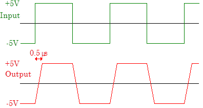 The maximum rate at which an op amp can change its output is called its slew rate. When fed a 10Vp‑p square wave, for example, an op amp with a 20V/$\mu$s slew rate (in a follower circuit) will change from one level to the other in 0.5 $\mu$s.
Slew rates are normally in the range of 1 to 1000V/$\mu$μ μ s. Though related, an op amp’s slew rate is not equivalent to its gain-frequency response. An op amp with a high small-signal frequency response at low amplitude may have a lousy slew rate, and would not be useful with high amplitude, high frequency signals.
Bipolar Junction Transistors
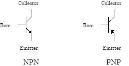 Bipolar junction transistors (BJTs) are the most common type of discrete transistor. Built with two adjacent junctions, bipolar transistors come in two flavors: NPN transistors consist of a p-type semiconductor layer sandwiched between two n layers, and PNP transistors consist of a central n-type layer sandwiched between two p layers. The central layer is called the base, and is the controlling lead. The two outer layers are the emitter and collector. BJT circuit schematics are shown to the right.
The two types are differentiated by the small arrow on the emitter, which indicates the direction of positive current flow in normal operation.
|
|
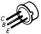
For the 2N2219 (NPN) and 2N2905 (PNP) transistors used in this lab, the emitter is the lead nearest the case tab, and the collector is the lead 180° from the emitter. The base is the lead in between. Note that the collector is connected to the case. Complete specifications for these transistors are available on the BSC web site.
The physics of bipolar transistors is much more complicated than that of field effect transistors, and we will not attempt to explain it here. Broadly speaking, BJTs are used in much the same way as FETs. The base corresponds to the gate, the emitter to the source, and the collector to the drain, and the base controls the current between the collector and the emitter. The primary difference between the two is that the BJT base, unlike the FET gate, draws current. In fact, the base-emitter junction looks like a forward-biased diode junction.[4] The base current makes BJT circuits and circuit analysis more complicated than FET circuits and circuit analysis. However, BJTs often have higher transconductance, smaller piece-to-piece variations, and, in some situations, lower noise than FETs.
For an NPN transistor, the collector voltage VC must be held positive with respect to its emitter voltage VE. If the base-emitter voltage VBE is approximately equal to +0.6V (the diode turn-on voltage), current will flow between the collector and emitter, but relatively little current will flow through the base. Base-emitter voltages much less than +0.6V will shut the transistor off (no collector-emitter current), and base-emitter voltages much larger than +0.6V will cause excessive base current, and likely burn the transistor out. PNP transistors behave like NPN transistors, but with all the polarities inverted: VC < VE, VBE » -0.6V, etc.
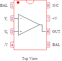
LF356
 |
The BJT follower and push-pull circuits used in this lab can be analyzed by assuming that their transistors are off when |VBE| is less than 0.6V, and on when |VBE| is greater than 0.6V. More complicated circuits require more sophisticated transistors models. Very briefly, two such models are: 1. The BJT as a current amplifier: the collector current $I_C$ equals a constant $\beta$ times the base current $I_B$, and the emitter current $I_E$ equals $I_B+I_C=(1+1/\beta)I_C$ . Beta depends on the particular model of transistor and is typically in the range 50 to 200. 2. The BJT as a transconductance amplifier: $I_c=I_S\exp{\left(qV_{BE}/KT\right)}$, where $I_S$ is a temperature dependent constant for each transistor. This model is called the Ebers-Moll model and, with some additional bells and whistles, is the model used in Spice. |
In the lab
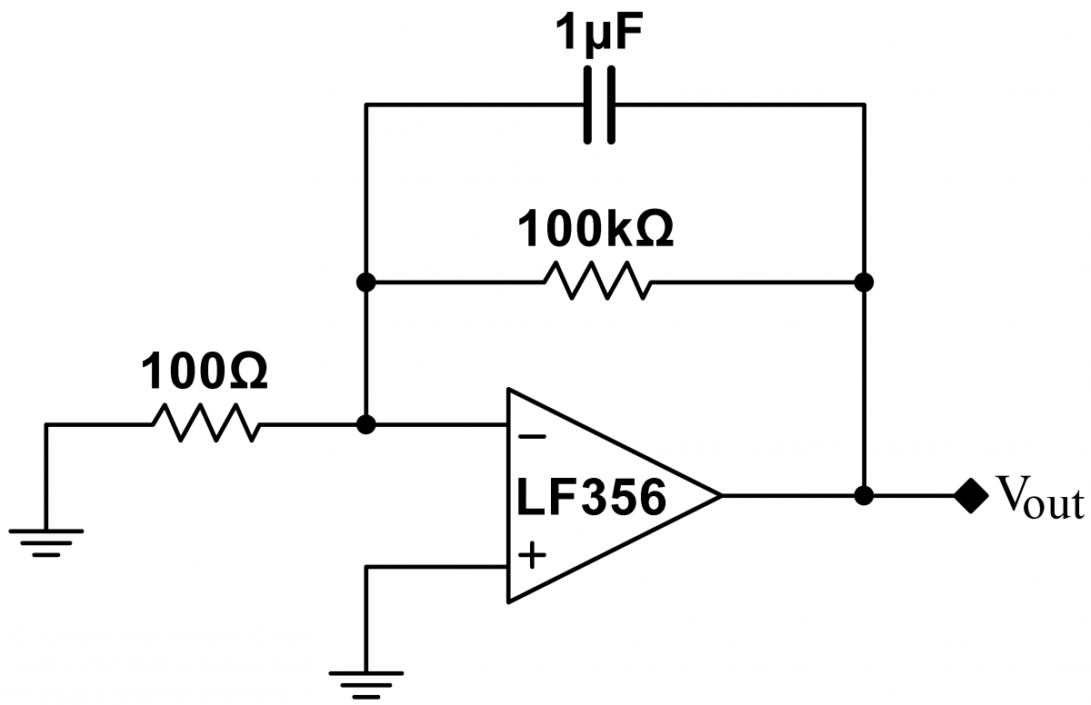
Problem 8.1 - Input Errors
|
Build the $\times 1000$ inverting amplifier shown at right. Note that the amplifier's input is grounded, so, if the op amp was ideal, its output voltage would be zero. (The $1\,\mu\mathrm{F}$ capacitor suppresses $60\,\mathrm{Hz}$ noise which would mask the effect being measured, but otherwise has no effect on the circuit.) Measure the circuit's actual output voltage. This error is called the “input offset voltage, $V_\mathrm{os}$. This circuit has a high gain. Input errors are always reported relative to the error at the input; the error is a function of the op amp, not of the circuit in which the op amp is embedded, so divide your measured output voltage by the circuit gain to calculate the input offset voltage $V_\mathrm{os}$ for this op amp. To get some sense of the variation between opamps, measure and record $V_\mathrm{os}$ of at least four other op amps. Watch how the offset drifts with time (just use the aproximate initial offset for comparison purposes). Is this a temperature effect? Investigate with circuit cooler. |
 |
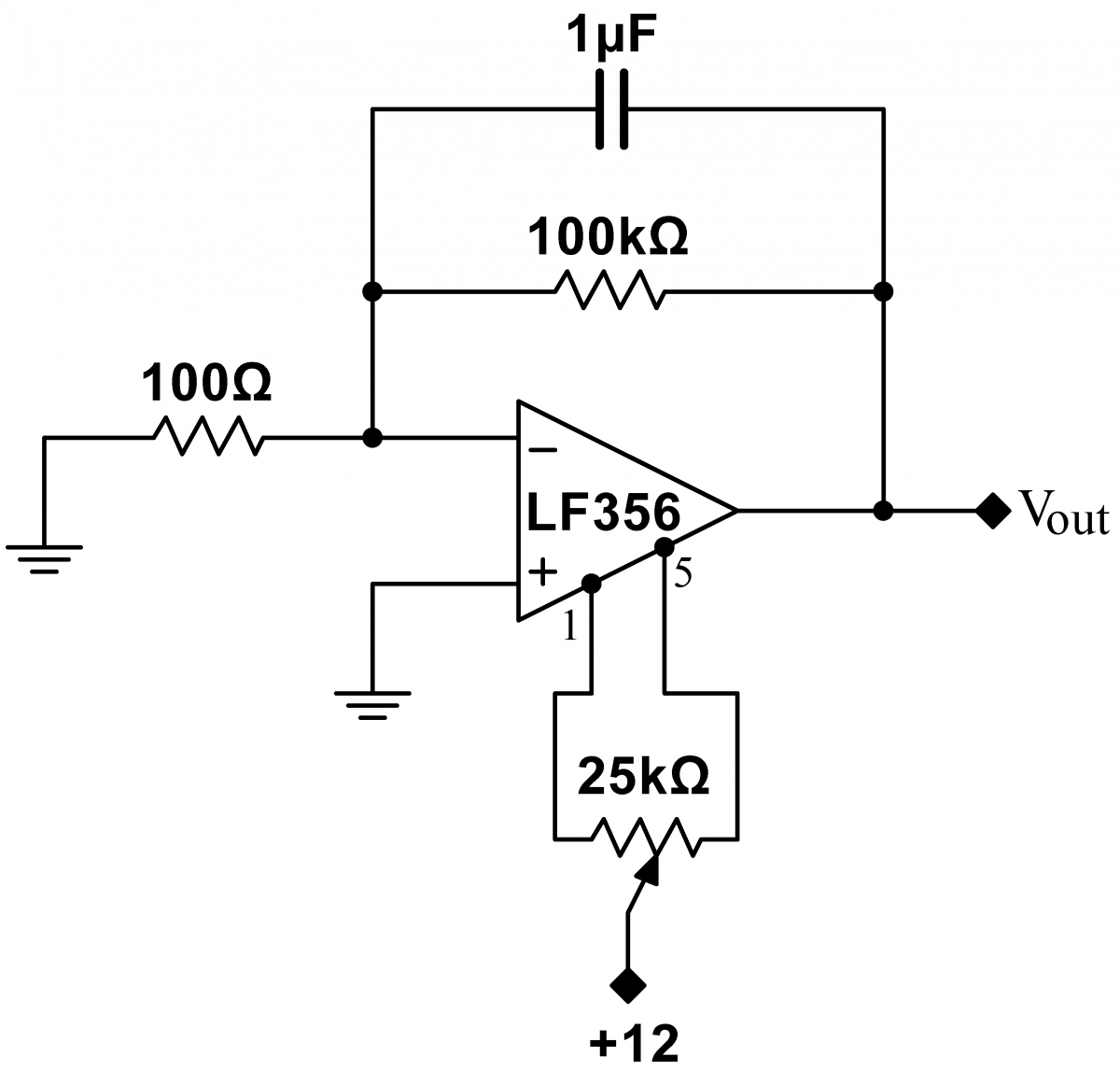
Problem 8.2 - Balance Adjustment
|
Pick an op amp with a relatively high drift. Build the circuit at right, which significantly decreases the input offset voltage $V_\mathrm{os}$ by "trimming" the op amp with a potentiometer connected between the two balance pins 1 and 5. (These pins are sometimes called the trim, null or offset pins.) Minimize the input offset voltage by adjusting the trimming potentiometer. How low can you get the offset? After adjusting, watch the output for several minutes. Does the output drift? The LF356 use JFETs in its input circuitry. Like most FET (both JFET and MOSFET) op amps, the LF356 has a relatively high offset voltage, and relatively high drifts. FET op amps would not be used in applications where these are are critical parameters. Bipolar op amps tend to have much lower voltage offsets and drifts. |
 |
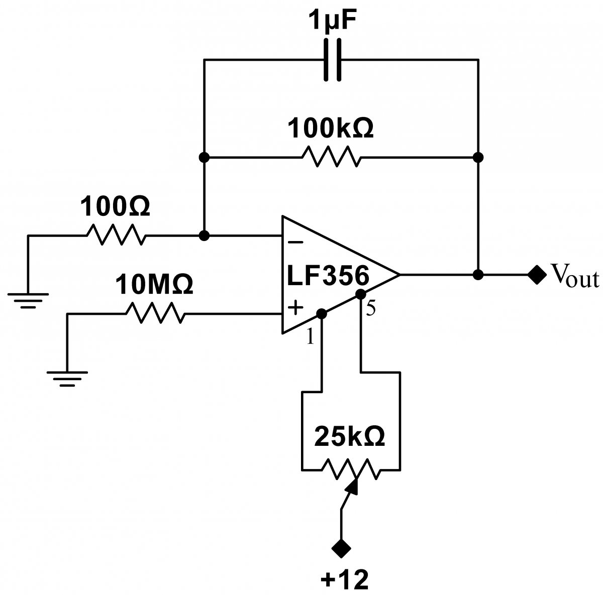
Problem 8.3 - Input Bias Current
|
The input bias current is a current that appears to come out of the op amp inputs. If this current is forced to run through a high resistance, an unwanted offset will appear on the output. Build the circuit at right to measure the input bias current $I_\mathrm{B}$. Begin by shorting out the $10\,\mathrm{M}\Omega$ resistor (leave the resistor in place), and trim $V_\mathrm{os}$ to zero. Record the approxmate average value of $V_\mathrm{os}$. Then remove the short and quickly measure and record the change in the output voltage. Calculate the input bias current from your measurement and from the resistance of the unshorted resistor. [Technically, this is an incomplete measurement, as it assumes that a related current, the input offset current, is zero. (This is a detail that you do not have to understand.)] As you should have just measured, JFET op amps have a relatively low current bias. With high impedance signal sources, JEFT and MOSFET op amps are superior to bipolar op amps. However, bipolar amps generally have a lower input offset voltage; there is not one best op amp for all applications. |
 |
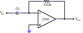
Problem 8.4 - Closed Loop Op-Amp Gain Frequency Dependence
|
Build the $\times1000$-inverting amplifier circuit at right. We will measure this circuit's closed loop gain as a function of frequency (closed loop gain means the gain at the output with feedback applied). Because the amplifier's gain is so large, it must be driven with a very small signal. As the signal generator cannot be adjusted to produce sufficiently small signals, use the voltage divider to reduce a $1\,\mathrm{Vpp}$ sine signal to $1\,\mathrm{mVpp}$signal. Measure the gain and phase for frequencies in the range of $10\,\mathrm{Hz}$ to $10\,\mathrm{MHz}$. Plot your results. |
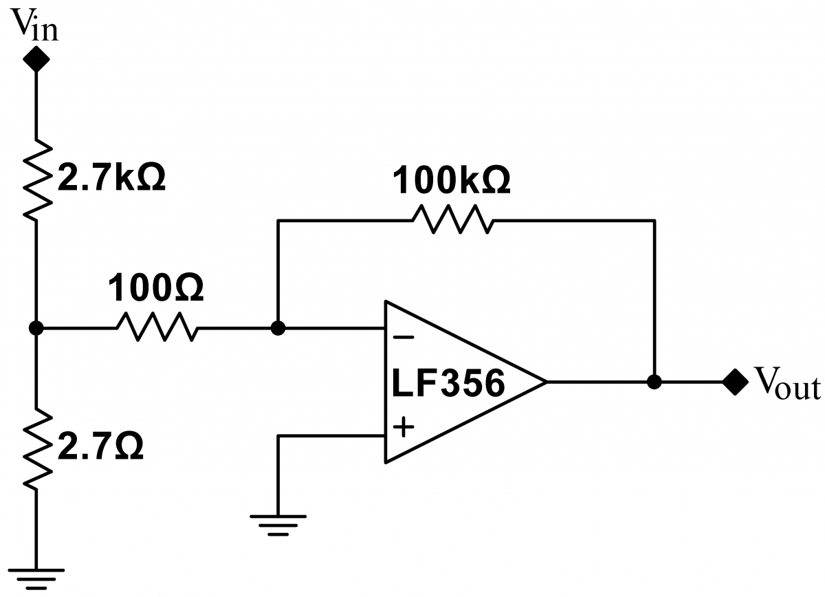 |
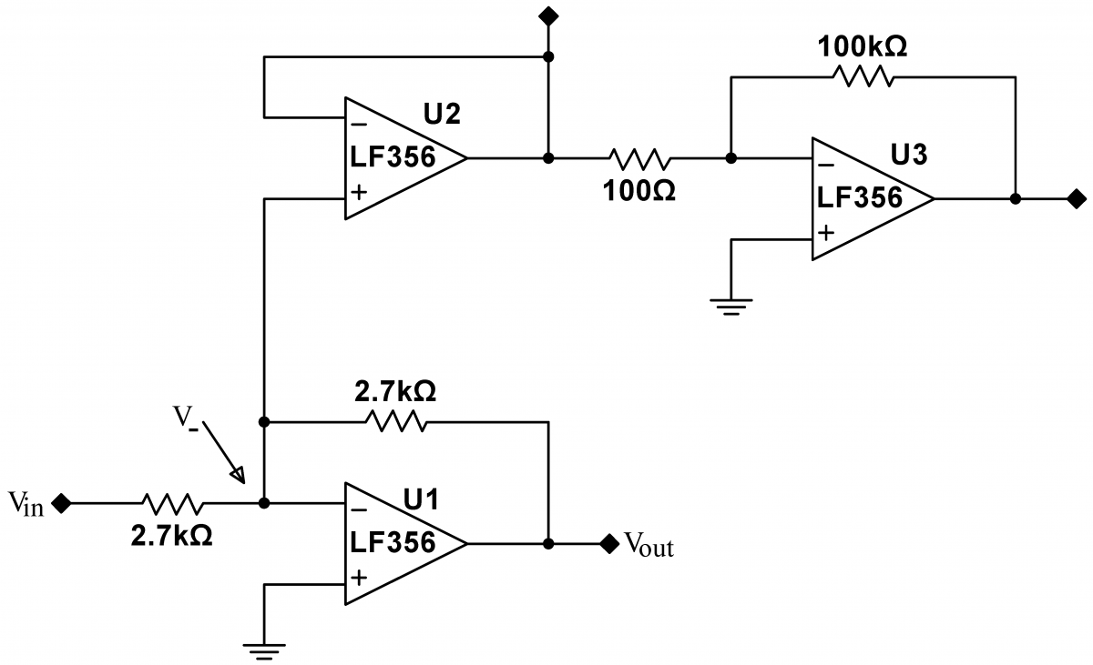
Problem 8.5 - Open Loop Gain
|
The open loop gain of the LF356 is very high, and is difficult to measure. (The open loop gain is the intrinsic gain of the op amp ignoring any feedback.) We will measure the open loop gain of op amp U1 in the circuit at right, which uses op amps U2 and U3 as amplifiers to make the open loop gain measurable. (By convention, op amps are often labeled with a U followed by a number.) Build the circuit at right, and drive it with a $1\,\,\mathrm{Vpp}$ sine wave. The open loop gain can be calculated from the formula $\displaystyle G_0 = \Bigg|\frac{V_\mathrm{out}}{V_+-V_-}\Bigg| =\Bigg|\frac{V_\mathrm{out}}{-V_-}\Bigg|$, where $V_\mathrm{out}$ is the output of U1, and $V_-$ is indicated by the arrow. Measure the open loop gain for frequencies in the range of $10\,\mathrm{Hz}$ to $10\,\mathrm{MHz}$. The open loop gain is extremely high at low frequencies, and therefore $V_-$ is extremely small. Use the amplifier chain U2 and U3 to amplify $V_-$ to a measurable value. You may have to increase the gain of U3. Note that the offsets studied in the earlier exercises will produce DC offsets in the measured signal. Ignore these DC offsets; measure only the peak to peak oscillating signals. At frequencies above about $1\,\mathrm{kHz}$, U3 will fail to have proper gain (see exercise 8.4). However, the open loop gain will have fallen, so $V_-$ will be larger. Thus, reduce the gain of U3 to $\times 100$ to restore proper operation. You will have to decrease the gain again, to $\times 10$, at frequencies above about $10\,\mathrm{kHz}$.Above $100\,\mathrm{kHz}$, the gain of U3 will fail once more. Here, use the output of U2 directly. Use scope probes for all your measurements. You may find that at low frequencies like $10\,\mathrm{Hz}$, your signal is masked by $60\,\mathrm{Hz}$ noise. Check to make sure that your signal really is related to your drive by turning on and off the signal generator. If the signal doesn't disappear with the signal generator off, then the signal is just noise. You can use averaging (use the maximum number of averages, 512) and external triggering to find the real signal. However, you will have to change the drive frequency to something incommensurate with $60\,\mathrm{Hz}$, say $11\,\mathrm{Hz}$. If you don't, the $60\,\mathrm{Hz}$ noise will be preserved by the averaging. What is the function of U2? |
 |
Problem 8.6 - Output Errors
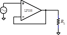 Drive a follower with a 10Vp‑p, 1kHz triangle wave.
Adjust the load resistor RL until you see the effect of the op amp’s finite output current. Draw the resulting output. Using several different load resistors, measure the maximum output current. Does it depend on RL?
Problem 8.7 -Speaker Driver
Obtain a speaker from the laboratory staff, and drive it with the following amplifier.
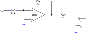
Handle the speaker carefully! The black-paper speaker cone tears easily. The 51$\Omega$ resistor protects the speaker, which will burn out if driven with more than about 0.2A. Drive the amplifier with the wavefunction generator, and look at the output on the scope. What do sine, square and triangular waves sound like? What is the maximum amplitude with which you can drive the speaker without distortion? Why? How does the output amplitude distort when you exceed that amplitude? Is the speaker loud? Switch the input to the T2 line, which provides an audio input signal. Is the quality acceptable?
Optional: In this and subsequent exercises, you may improve the sound volume and quality markedly by mounting the speaker on an inside wall of a cardboard box. At the location of the speaker, cut a hole in the box wall matching the diameter of the speaker cone. Even a small box, or any such enclosure, will be benificial.
Problem 8.8 Bipolar Follower
The output current limit can be increased by using the op amp to drive a bipolar follower.
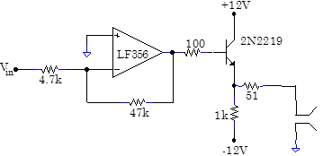
With a sine wave input, how does the output change as the input amplitude is varied from 0.01V to 1V? Draw all the qualitatively different output waveforms that you observe. Does the speaker emit a pure sine note at all amplitudes? What is the sound quality when the amplifier is driven by T2?
Problem 8.9 Bipolar Follower in Feedback Loop
The follower’s performance can be improved somewhat by including the follower in the feedback loop.
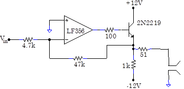
How does the output change as the input amplitude is varied from 0.01V to 1V? What sort of input waveforms would this circuit amplify without distortion?
Problem 8.10

The Multisim schematic FollAmp (located in BSC Share/Multisim/Lab8) compares circuits 8.8 and 8.9. Simulate the schematic for input amplitudes of 0.01, 0.05 and 0.25V. Explain all the differences between the waveforms including: (1) The large offset at 0.01V for 8.8’s circuit. (2) The smaller offset at 0.01V for 8.9’s circuit. (3) The half wave distortion for both circuits at 0.25V. (4) The improved performance of 8.9 over 8.8 at 0.05V.
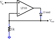
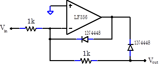
 Problem 8.11 Pushpull Driver
A “push-pull” output stage performs much better than a follower output stage.
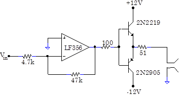
Look at and listen to the output for a variety of input signals. For 500Hz, 0.015Vp‑p, 0.15Vp‑p and 1.5Vp‑p sine waves, examine the “crossover distortion” where the output crosses zero. What is the origin of the crossover distortion?
Now include the push-pull output stage in the feedback loop.
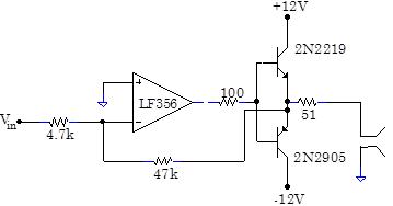
Has the crossover distortion diminished?
With the T2 audio signal, change the feedback point back and forth between the op amp output and the push-pull output. Can you tell the difference in the sound quality?[6]
Slightly more complicated push-pull amplifiers can be designed that have very little crossover or other distortion. Push-pull amplifiers are extremely common, and are found everywhere from the output of op amps to the output of power stereo amps.
Problem 8.12 - Noise
Measure the LF356’s voltage noise with the following circuit. You will need to borrow a commercial preamp. You should ask lab staff for the preamp.[7]
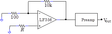
Set the preamp gain to 100, its low-pass filter to 100kHz, and its high pass filter to 1kHz. Measure the RMS noise from the op amp alone by setting R = 0. You can use the RMS function on the digital multimeters, but there is a useful way of guessing the RMS voltage: Watch the noise on the scope, and get some sense of the maximum peak-to-peak signal. It turns out the RMS signal is approximately equal to the typical maximum peak-to-peak signal divided by six. Try it both ways.
Now measure the Johnson noise generated by a resistor by setting R = 1M. Once again, find the RMS level. If you can find a sine wave on the scope, you are not measuring Johnson noise, you are measuring pickup on a large impedance in a noisy environment.
Problem 8.13
Explore different types of noise with the LabView program Noise Generator. Start by setting the program to “Gaussian White Noise” and “Generate Real Time Data”. Hit the “Generate” button, and the program will generate a set of gaussian distributed data points, display their spectrum, and play the resulting signal through the speakers. Take a look at the amplitude histogram in the lower left corner; as expected, the noise is Gaussian. Generate several new data sets, and note how they all sound alike. Then change the settings to “Generate Spectrum”, and generate a new data set.[8] Here the program first generates a gaussian distributed spectrum, and takes an inverse Fourier transform to find the real time data, which it then plays over the speakers. Is the amplitude histogram still gaussian? These two methods of generating noise are formally identical. Also try “Uniform White Noise”, which generates uniform distributed noise instead of gaussian distributed noise. These two types of noise are quite different mathematically, but sound almost the same.
Change the settings to “1/f Noise”, and generate some data sets. Listen carefully: doesn’t the noise sound like a distant ocean waves? As you can see in the spectrum graph, the amplitude of the frequency components in 1/f noise are inversely proportional to the frequency. 1/f noise is very common in nature, and can be used to model phenomenon as disparate as the curvature of a beach to the volume produced by a symphony orchestra to the spectrum of noise from almost all semiconductor devices at low enough frequencies. The prevalence of 1/f noise is one of the deep questions about our world; nobody has a good explanation for its ubiquity.
You might think that 1/f noise is similar to bandwidth-limited white noise, but it actually sounds quite different. Go back to the “Gaussian White Noise” and “Generate Spectrum” settings, but this time set the low pass frequency to 500, i.e. 500Hz, and listen to the sound. This will produce white noise whose maximum frequency is 500Hz. It is quite different than 1/f noise…more like the noise of a furnace. Can you explain why?
Set the noise generator to “Shot Noise”, and the “Average Number of Shots per Sample” to 0.001. Shot noise is also called counting or Poisson noise, and occurs whenever as an average number of samples is supposed to arrive in a fixed time interval. An example is the number of electrons per second that cross a fixed point in a wire carrying a “constant” current. Despite the fact that the current is supposed to be constant, there will be random fluctuations in the number of electrons. Another example is the number of radioactive decays in ten seconds from a radioactive sample. On the average, say, ten decays might be expected, but the number in any given ten second interval will fluctuate. The size of the fluctuation is proportional to the square root of the expected number of samples: if you expect an average of N counts, the average fluctuation will be ![]() . Note that the normalized number of fluctuations,
. Note that the normalized number of fluctuations, ![]() , decreases as N increases.
, decreases as N increases.
Now generate a shot noise data set. What does it sound like? Change the “Average Number of Shots per Sample” to 1. Generate a new data set. What does it sound like? Try setting the “Average Number of Shots per Sample” to 100 and 10,000. See how the amplitude histogram becomes gaussian? Is this consistent with the sound that you hear? Note that the data set is normalized; can you explain why the sound volume decreases at high “Average Number of Shots per Sample”?
Finally, change to “Line (60Hz) Noise”. Generate some data sets, and play with the “Harmonic Content” knob. Where have you heard this sound before?
Problem 8.14 - Frequency Errors
|
Run the Multisim schematic “DirectGn”, and record the gain and phase shift of the LF356 as a function of frequency. |
Problem 8.15
Construct the differentiator below. Make sure that you use decoupling capacitors. Show, using the golden rules, that this circuit should differentiate.
Ground the input and look at the output. Unfortunately, the circuit is unusable because it oscillates spontaneously. If it doesn't oscillate, drive it with a square wave and you should see it ring. Measure this oscillation or ring frequency. Why does the circuit oscillate? Hint – What is the amp’s phase shift at the oscillation frequency (see 8.14)? What is the phase shift of the feedback network?
Problem 8.16
Construct the practical differentiator below.
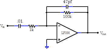
Why is it stable? Record the output of the differentiator for a variety of input signals. Sketch the Bode plot. Does the circuit differentiate at all frequencies?
Problem 8.17
Drive an op amp follower with a 200kHz, 10Vp‑p square wave. Draw a picture of the follower’s output. What is its slew rate?
Problem 8.18
The followers in 8.8 and 8.9 cannot drag their outputs very negative. Can this problem be cured by decreasing the follower’s emitter resistor, say from 1k to perhaps $51\,\Omega$? Hint – This fix works in Multisim, but will not work in the real world..
How does the push-pull circuit (8.11) get around this problem?
Problem 8.19
|
Calculate the gain of an inverting amplifier assuming that its op amp has finite open-loop gain. Using your open-loop gain data from 8.14, or 8.5, can you correctly predict the gain in 8.4 as a function of frequency? |
Problem 8.20
Diode rectifying circuits like those in Lab 4 are not accurate because of the 0.6V diode turn-on voltage. Better rectifying circuits can be constructed with op amps, but are complicated by finite slew rates
Build the simple active rectifier circuit below.
Drive it with a triangle wave, and look at its output. At 1kHz the circuit should work quite well, but at higher frequencies the output will be distorted. Draw the distorted output signal. Now look at the output of the op amp itself, and draw what you see. Can you explain why the op amp’s finite slew rate degrades the performance of the circuit? Hint—take a look at the output of the op amp.
A much better rectifying circuit can be constructed as shown below.
Verify and explain why this circuit works better.
Student Evaluation of Lab Report
After completing the lab write up but before turning the lab report in, please fill out the Student Evaluation of the Lab Report.
Appendix: Op Amp Compensation
Op amp frequency and phase behavior is quite complicated. All op amps consist of several gain stages, and the gain of each stage will decline at high frequencies because of parasitic capacitances inside the stage’s transistors. The op amp can be modeled as a perfect, frequency-independent, high-gain differential amplifier, followed by a series of active low pass filters, each filter representing the frequency response of one stage of the op amp.
The stages acts successively; the net gain is the product all the gains, and the net phase shift is the sum of all the phase shifts. The low-pass cutoff frequency for each stage is similar, typically around 10MHz. Remember that the phase shift of an RC filter driven above its cutoff frequency approaches 90°; thus the net phase shift at sufficiently high frequencies will cross 180° on its way[9] to 270°. At the 180° crossing point, the inverting input effectively becomes a noninverting input, and the feedback, which is hooked up to the now noninverting V- input, changes from positive to negative. Like any other circuit with positive feedback, the amplifier will oscillate if the gain is greater than unity.
Careful analysis of a high gain op amp whose low-pass cutoffs are all at approximately the same frequency shows that the gain is indeed greater than unity at the 180° crossing point, and the op amp will oscillate. To prevent oscillations, most op amps, including the LF356, are “compensated”. A compensation low-pass filter is added to insure that the gain is less than unity at the 180° crossing point.
The compensation filter must be designed to cut in at a quite a low frequency: typically at less than 100Hz. The frequency response of the op amp is almost entirely set by this compensation filter.
As it significantly degrades the frequency response of the op amp, compensation is a steep price to pay for stability. Compensation also decreases the amp’s slew rate. Detailed analysis of the stability problem shows that oscillations are hardest to avoid for unity gain followers; high gain amplifiers are much less likely to oscillate. Special uncompensated op amps are available which have both higher frequency responses and faster slew rates, but can only be used in high gain circuits. Some op amps are available in both compensated and uncompensated forms; for example, an AD849J is an uncompensated version of the compensated AD847J. AD849Js are only stable when used with gains greater than twenty-five, but are about fifteen times faster.
[1] Audio white noise sounds like the sound from an ocean or highway so distant that the noise from individual waves or cars is not distinguishable. Audio white noise is innocuous, peaceful even. For example, aircraft cabins are full of rather loud white noise; think about how loud you have to talk to converse with someone two rows away. Yet it is possible to sleep on airplanes because the noise contains few distinguishable sounds. The phone company takes advantage of white noise’s innocuous nature by deliberately adding white noise to phone lines to mask annoying pops, crackles, and other distinguishable noises.
[2] Bipolar op amps also exhibit current noise, random fluctuations in IB and Ios.
[3] Einstein showed that fluctuations or noise are intrinsic to any system that exhibits dissipation. Thus any component with resistance (resistors, transistors, etc., but not capacitors or inductors) will necessarily be noisy.
[4] As opposed to a reversed-biased diode junction in a JFET.
[6] Your answer probably depends on whether your audio signal is rock or classical music. So much distortion is deliberately added to rock music that there is little point to using a high quality amplifier.
[7] Probably the SRS 560 Pre-Amp. We use a commercial preamp rather than constructing our own preamp because the commercial preamp has a built in bandpass filter.
[8] Make sure “Low Pass Frequency” is set to11.03E+3 (11.03kHz).
[9] In our example there are three stages. Hence the net phase shift is three times 90°, or 270°.
$V_\mathrm{os}$