Digital Circuit Elements I
University of California at Berkeley
Donald A. Glaser Physics 111A
Instrumentation Laboratory
Digital Circuit Elements I
Copyrighted ©2014 The Regents of the University of California. All rights reserved.
| Reading: | ||
| Horowitz & Hill | Chapter 8 | |
| Sedra and Smith | Chapter 13 (Sections 13.1-13.7) | |
| Millman & Grabel | Chapters 7 and 8 |
Physics 111-Lab Library Reference Site
Reprints and other information can be found on the Physics 111 Library Site.
In this week’s lab you will learn the basics of digital circuits, including digital logic, (TTL) switches, flip-flops, and counters.
NOTE: You can check out and keep the portable breadboards, VB-106 or VB-108, from the 111-Lab for yourself ( Only one each please)
Pre-lab
1. Simplify the following Boolean expressions (‘0’ stands for false, ‘1’ stands for true):
(a) 0 · 1, (b) 0 + 1, (c) 1 · 1, (d) A(A + B), (e) ![]()
2. Show that ![]()
(a) using truth tables and (b) using logical manipulations.
3. An “eXclusive-OR” or “XOR” gate outputs “true” only if exactly one input is true. Write the Boolean expression describing the XOR of two inputs A, B. Prove using Boolean algebra that the circuit shown in Section 10.4 represents an XOR.
4. Write the integers 0-15 in decimal, binary, BCD, and hexadecimal (a.k.a. “hex”). For numbers less than 10, BCD is the same as binary. BCD means that each digit of a number is individually coded as a binary number, rather than the number as a whole.
5. Calculate the truth table for the circuit in 10.6.
NOTE: You must tie the open inputs on TLL to low or high (not open) when X is in the truth table.
In the lab
You should obtain a set of digital chips and a breadboard that you can take home from the staff. Show your syllabus card and sign out a complete set of chips and keep it until the end of semester. If you find that you have a bad chip or if you burn one out, see a staff member for a replacement at no charge. (Initial packages come with working chips.)
Special notes:
Digital circuits can be built in different technologies: DTL, TTL (S & S sections 14.3 and 14.4), CMOS (S & S chapter 13.6), ECL, etc. Each is best suited to different applications, but the principles of use are common to all. In this lab we use TTL (transistor-transistor-logic). This family of logic circuits requires a 5 V supply voltage and will burn up quickly if +12 V or –12 V are applied. Before using any TTL chips, check the voltage put out by the 5 V power supply.
Typical characteristics as well as the pin assignments of TTL chips can be found in the TTL data book. Generally, TTL circuits accept voltages around 0 V as ‘low’ and voltages around 5V as ‘high’ (see TTL-Data Book for detailed specifications); it is therefore alright to connect an input directly to ground or +5 V. Do not leave inputs floating: always tie them to either 0 or +5V.
Hints:
It is a very good idea to disassemble a circuit only after you are sure you are done with it. The reason we check boards out to you is precisely for this reason so you don’t have to take anything apart—many of your later circuits will be based on earlier–built circuits, so you'll want to still have them.
Also, there is usually more to do to get a circuit to work than what the lab manual indicates. For instance, feeding a square wave to a particular input on a chip will not be enough to make the chip work even though this is the only connection shown. We rarely mention that all gates, counters, etc. need power connections, and often there are presets, resets, enables, etc. that need to be tied high or low, as appropriate, or the chip just won’t work. These are things you should look for when examining the specification sheets. Unlike the previous analog circuits, it is unlikely that you will make any progress in the lab if you haven’t read up on these chips in the data books or appendices.
Note: in the following, the +5 V state of an input or output is called ‘high,’ ‘true,’ or simply ‘1;’ the 0 V state is called ‘low,’ ‘false,’ or simply ‘0.’
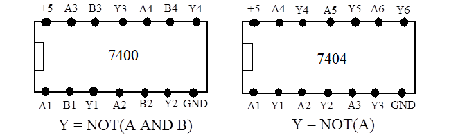
Figure 10.1 Top view of NAND, 7400 and the Inverter, 7404 chips
Problem D1.1 - TTL Transfer Characteristics
Study the transfer characteristics of a TTL – NAND gate using a 7400 chip. Connect one input to +5 V, the other to a triangular wave oscillating between 0 and +5 V. Use the DC offset (level shifter) circuit to get the required input. Display the transfer characteristic on the scope, using the xy-mode and connecting the input signal to x (Channel 1), the output to y (Channel 2). What levels are considered ‘low’ and ‘high’ in TTL circuits (see data book)? For which range of inputs is the NAND output ‘low?’ For which range is it ‘high?’ Does the characteristic change if a load (i.e. the input of another gate) is connected to the output?
Since the offset adder is too slow for this signal (why?), you’ll need to drive the gate directly from the Wavetek generator. Think carefully about what voltage to use when measuring the delays and explain your choice. (Hint: If you cascaded 100 gates the delay should be 100X your single gate measurement). Using the normal, non-xy-mode of the scope, use a 1 MHz square wave input to measure the propagation delay of the gate.
Problem D1.2 - Basic Gates
Verify the truth table for one of the NAND gates in the 7400 chip, and verify the truth table for one of the inverters in the 7404 chip. You should never leave inputs open because these states may flip when you don't want them to. Using the 7404 and the 7400, conclude which states these are, high or low, when you do leave them open.
Problem D1.3 - Basic Digital Functions and Boolean Algebra
Using DeMorgan’s theorem where appropriate, construct (a) an inverter, (b) an AND gate,
(c) an OR gate, and (d) a NOR gate out of NAND gates. In each case, try to use the minimum number of gates. Build the circuits and test their truth tables.
 Problem D1.4
An “eXclusive-OR” or XOR gate outputs “true” if exactly one input is true. Build the following circuit (figure 10.2), and verify that it acts as an XOR gate.
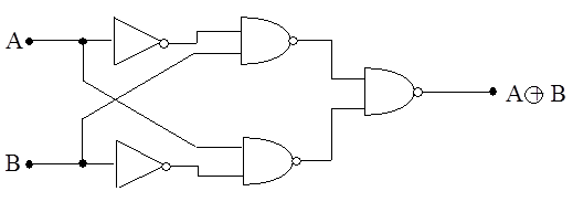
Figure 10.2 An exclusive -OR circuit
Problem D1.5
The 74151 chip is an 8-input multiplexer. A multiplexer is a circuit element which has several input data lines, two data output lines, and an address register. Our chip has 8 input lines and a three-digit binary number address register that determines which of the 8 data inputs is connected to one of the output lines. The second output line is automatically made the complement of the first output line. Hook up the 74151 and spot-check its operation. How can you use it to generate an arbitrary 3-input truth table? Write out the truth table for inputs A, B, and C of a 3-input XOR. Wire and check a circuit which gives a 3-input XOR.
Optional Problem
Using this chip and one additional inverter it is actually possible to generate arbitrary 4-input truth tables. Explain how, then build and verify the operation of a 4-input XOR.
Flip-Flop
For all the circuits discussed above, the output at any time depends only on the inputs at that time, and not on the state of the inputs at any previous time; the circuits have no memory. In the following, we shall try circuits where the output depends on the history of the circuit. The simplest of these is the flip-flop, also known as the FF or just ‘flop'.
Problem D1.6
Build the following circuit and measure its truth table (note: the output Qn+1 at time n+1 depends on the inputs An+1 and Bn+1 and on the previous value Qn of the output).
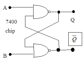
Figure 10.3 A simple flip-flop circuit with only one output Q
One application of a flip-flop is as a de-bounced mechanical switch. When you close an SPST (“single-pole, single throw” – one wire which can be connected to one contact) switch [see Figure 10.4(a)], the output voltage does not change instantly, as expected for an ideal switch [see Figure 10.4(b)]; instead, the switch tends to ‘bounce’ (one contact physically bounces on another, making and breaking the connection rapidly many times) and the output looks like Figure 10.4(c). You should look at this output, which is straightforward to do with a properly trigged oscilloscope.
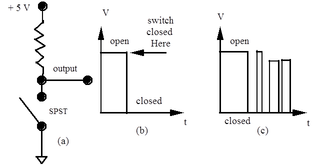
Figure 10.4 An SPST switch with (b) ideal performance - when switch is open, logic level = 1; switch closed, logic level = 0, (c) observed waveforms due to bouncing of switch contacts.
Such a switch is obviously not appropriate in circuits which count the number of input pulses or falling edges; closing the switch would cause several counts instead of just one. One solution is to build the circuit shown in Figure 10.5 using a SPDT (“single-pole, double-throw” – one wire which can be connected to two different contacts) switch and add a flip-flop (a 7400 chip) to ‘de-bounce’ it. Explain how this works, and verify that it works as expected.
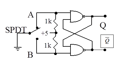
Figure 10.5 De-bounced Switch circuit
Problem D1.7
Using a few more NAND gates, one can create a flip-flop whose output is toggled between true and false with each pulse at the ‘clock’ input. The 7490 decimal counter contains such flip-flops. It consists of four flops — the first, 'A' flop, is unconnected to any others and is directly accessible for your use. The other three, B through D, are wired together in a more complicated fashion. Build the circuit using the de-bounced switch shown in Figure 10.5 and connect the output 'Q' to the input of the 'A' flop of the 7490 (clock input at pin 14, output at pin 12). Study the operation of the 'A' flop. Make sure you have the 7400 and the 7490 chips wired correctly. What is the effect of the R0 and R9 inputs of the 7490? Does the output of 7490 (pin 12) change with the rising or the falling edge of the clock signal (pin 14)?
Today you can buy a de-bounced switch as a chip placed inside or outside of the mechanical switch itself.
Problem D1.8
Although flip-flops can be synthesized from two NAND gates, it is far more common to use prepackaged flip-flops. Construct the circuit below, driving it with a 5V p-p square wave from the signal generators. Start with a signal frequency of a few Hertz. The LEDs should blink on and off. What is the frequency of the output LED relative to the input LED?
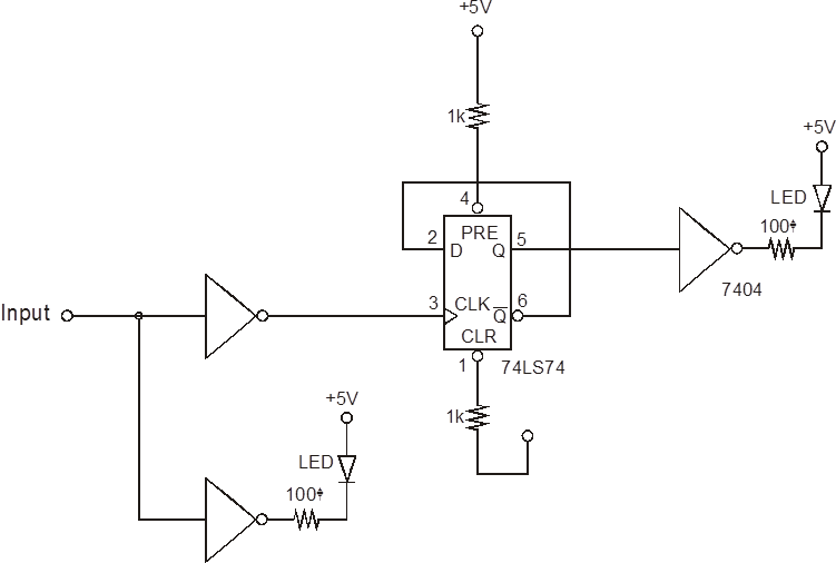
Now set the frequency generator to 10kHz. Does the 74LS74 switch on the leading or trailing edge of the clock signal? Increase the signal frequency. What is the maximum frequency at which the circuit still switches the gate appropriately? Do you get a nice, clean waveform at frequencies just below the maximum?
Try driving the circuit with the waveform generator sync output instead of the normal output. Set the signal generator at 10kHz, and look at both the input and the output. Can you explain what you see on the scope?
Note that the preset and clear inputs are tied to +5V through a resistor. This allows these inputs to be shorted to ground without shorting the power supply. What happens when you short each input?
Finally, why are the LEDs buffered through an inverter rather than connected directly to a signal lead? Hint---take a look at the signal at the LED cathodes.
Problem D1.9 - Counters
Since the output of an appropriately connected D-type flip-flop makes a true-false transition with every second true-false transition of its input signal, it acts like a divide-by-two circuit. Several such flip-flops can be cascaded to form a binary counter. With a few additions, the circuit can be reset with each 10th pulse. A typical decimal counter is the 7490. By consulting the spec sheets, figure out how to hook up a 7490 to make it count. You will need to connect the output QA to the input B. Then reset the counter and watch it count 0-9 and start again at 0. [Hint: Study the spec sheets for this chip carefully. You must make sure that every pin is connected to an appropriate value.] You will get more consistent results if you clock the counter using a de-bounced switch.
Optional: Is it possible to get the counter to count backwards? Build such a circuit, and have this section signed by a staff member.
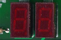 Observing the output of the counters on the oscilloscope is awkward. It would be far more convenient to display the counter output with LED digits, similar to those found in some watches. The FND357 is a 7-segment LED display capable of displaying all digits and a few letters. Each of the seven lines in the FND357 picture at right is an individually controllable LED. The 9368 is a 7-segment decoder driver chip that can take the output from your counter chips and convert it into the proper driving voltages for the FND357.
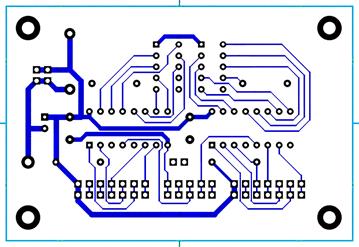
Hooking up the 9368 to the FND357 takes quite a few wires, and is a pain to get right. Moreover, wiring the circuit on a breadboard is obviously inappropriate for a commercial circuit. To illustrate how commercial circuits are manufactured, we have wired the 9368 to the FND357 on a commercial-quality printed circuit board (PCB). A PCB is a stiff board (normally made from epoxy stiffened with some fibers) on which the wires (or traces as they are normally called) are made from thin, flat copper foil glued to the epoxy board. The finished board is pictured below:
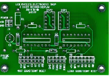
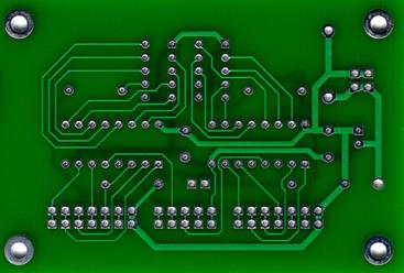
Front View Back view
The traces are the light green (gray in black and white) lines and are present on both the front and the back of the printed circuit board. Note that the traces on the same layer are un-insulated from each other. This makes designing printed circuits something of an art as it is not always easy to wire an entire circuit without having wires intersect. Fortunately the wires on the front and the wires on the back are insulated from each other, so it is possible to have insulated intersections on different layers. (Sometimes two layers are not sufficient. The main circuit boards inside a computer (called the motherboard) may consist of four different epoxy boards sandwiched together.)
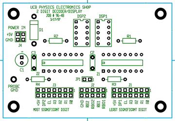
Once the board is made, it is “stuffed” with the necessary components, i.e. the component leads are pushed through the holes in the board. (The holes are difficult to discern in the pictures above, but are the regularly spaced rows of holes.) Next the components are soldered into place. Soldering complex boards by hand is too slow and prone to too many errors; typically the boards are soldered by literally floating them on a bath of molten solder. Only the bottom of the board needs to be soldered explicitly as the solder will flow up from the bottom layer to the top layer. Our completed board is shown to the right:
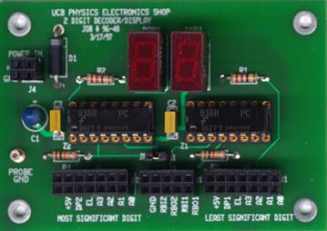
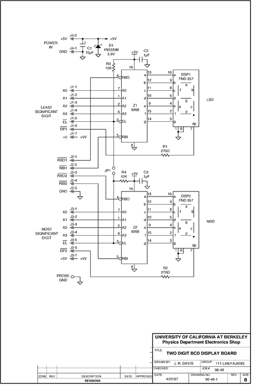
The process of creating a printed circuit board begins with a tested and debugged circuit. (The testing and debugging may well have been done with a breadboard similar to ours.) The circuit diagram used for our circuit is shown below:
Finished Circuit
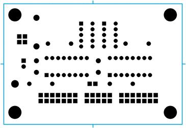
Next, the circuit wires are “layed out”. Laying out means finding the wire or trace pattern that makes all the necessary interconnections between the circuit elements. A mask is created for each layer:
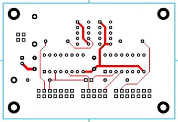
Top Mask Bottom Mask
The printed circuit board itself is made from a board which is initially coated with a solid copper layer. The masks are used to photo-lithographically etch the solid copper away, leaving the traces behind.
Holes for the component leads must be drilled through the epoxy board. The proper positions of the holes are specified in something called a drill list, which can be submitted to a machine that automatically drills the holes in the proper places.
 The traces are somewhat delicate. Moreover it is desirable to limit the solder to the places where the component leads are stick through the board and prevent the solder from flowing all over the traces. The solder mask is a transparent layer of paint that is applied to the printed circuit board that protects the traces and limits the solder flow. The solder mask is relieved away from the board holes so that the solder can adhere there. The solder mask is also applied lithographically with a negative mask:
Solder Mask
Note that the same mask can be used for both sides of the board.
Using a PCB without any labels identifying the input and output signals would be difficult. A final layer of paint, called the silk screen, is applied to the board to provide labels. The silk screen also shows simplified pictures of the components to aid in stuffing the board, and identifying information listing the purpose and manufacturer of the board.
Problem D1.10 - Silk Screen
Use your DMM to trace some of the traces on the PCB. Test the resistances between various pins and verify that pins connected by the trace are actually connected and random pins are unconnected.
Problem D1.11
Refer to circuit diagram and the 7490 specifications to figure out how to display the output of your counters on the display board. How many counts/switch do you observe?
Problem D1.12
Figure out how to cascade 7490s, i.e. to make the second 7490 count each time the first changes from 9 to 0. Get a second 7490 and try it out!
Problem D1.13
The 9368 provides some additional features: a blanking of leading zeros in multi-digit displays, and an internal buffer which can be used to freeze the display in a given state, whether or not the inputs change. This last feature is useful in devices like frequency counters, where the counter counts input pulses for one second and, while displaying the result, resets and starts counting again, in order to update the display after another second. Verify these features and test them.
Questions
1. Convert to decimal: 1110101.0110, 11.01010101, ADhex, and 258.
2. (Refer to Section 10.2) Based on the circuit diagram shown in Figure 10.6, explain how a CMOS AND gate circuit works.
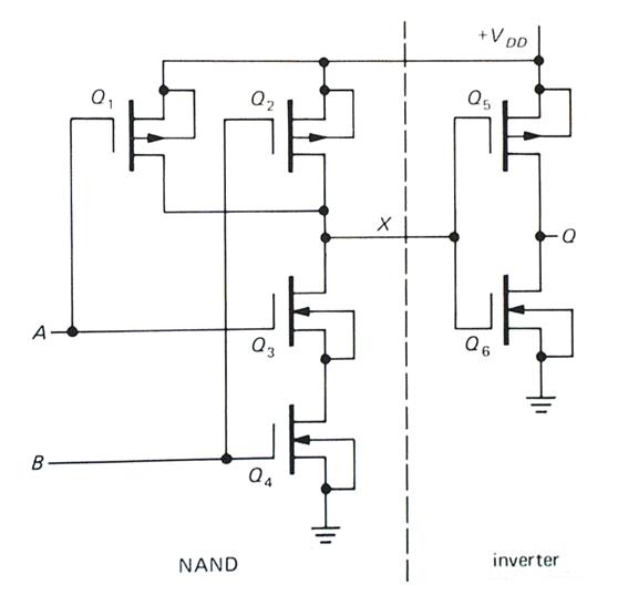
Figure 10.6 CMOS AND gate circuit
Student Evaluation of Lab Report
After completeing the lab write up but before turning the lab report in, please fill out the Student Evaluation of the Lab Report.