Digital Circuits II
University of California at Berkeley
Donald A. Glaser Physics 111A
Instrumentation Laboratory
Digital Circuits II
555 Timer, Analog-to-Digital (ADC) and Digital-to-Analog Conversion (DAC)
Copyrighted © 2014 The Regents of the University of California. All rights reserved.
| Reading: | ||
| Horowitz & Hill | Chapter 5.14 and 9.15-9.26 | |
| Hayes & Horowitz | Pages 214-215 and 406-415 | |
| Millman & Grabel | Pages 690-692, chapter 16.4-16.5 | |
| Senturia & Wedlock | Pages 526-535, chapter 18.3 | |
| Stubbins | Chapter 12 (see Appendix) | |
| Higgins | Pages 258-285 (see Appendix) | |
| Sedra & Smith | Chapter 10.9-10.11 |
Physics 111-Lab Library Reference Site
Reprints and other information can be found on the Physics 111 Library Site.
In this lab you will learn about the 555 timer chip and its varied applications. Your will also learn the basics of digital circuits, including digital logic, (TTL) switches, flip-flops, and counters.
NOTE: You can check out and keep the portable breadboards, VB-106 or VB-108, from the 111-Lab for yourself ( Only one each please)
Pre-lab
1. Explain the monostable and astable modes of the 555 timer qualitatively.
2. Derive the equations for the oscillator circuit based on the explanation given in Section 11.1 and in the specifications. Find the frequency and duty cycle of the circuit as functions of RA, RB,
and C.
3. Derive the equation for pulse duration in terms of R and C for the 555 in monostable mode (see Section 11.2).
4. What is an ADC? DAC?
5. How are these useful? What is Shannon’s sampling theorem? Give a short, plausible argument for this theorem.
General remarks: CMOS ADC and DAC chips are very sensitive to static electricity. Be sure to touch the conductive foam and the circuit ground before you remove the chips from the foam. Double check your wiring carefully before turning on power. In particular, check that the ADC is connected to the +5 V supply, in contrast to the DAC, which needs +12 V and –12 V. Input signals for the ADC must always be in the range 0 to +5 V (no negative inputs!). Check input signals using the scope (set to DC) before connecting them to the ADC.
In the lab
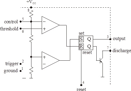 |
The 555 timer circuit The NE555 timer chip is a chip with a tremendous range of applications in digital circuits and analog-digital interfaces. |
| Figure 11.1 Schematic diagram of the NE555 timer chip |
Problem D2.1
The 555 can be used as an oscillator ("astable" mode) in the circuit shown in Figure 11.2:
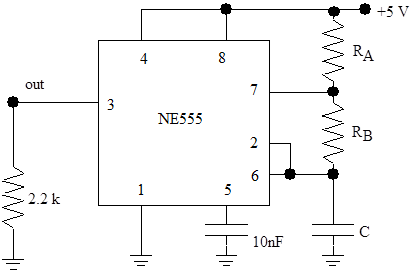  |
| Figure 11.2 NE555 oscillator circuit |
The circuit works as follows: initially, the flip-flop (‘flop’) in the 555 is set, and the discharge transistor does not conduct. C charges up via RA and RB until the voltage across the capacitor C reaches 2/3 of VCC. At this point, the upper comparator switches and the flip-flop is reset to low (L). The discharge transistor starts conducting and discharges C via RB, until the voltage at C falls below 1/3 of VCC, at which point the lower comparator (pin 2) switches and sets the flop again. Also see the specification sheets.
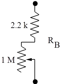
Build the circuit in Figure 11.2 using 2.2 kW for RA, another 2.2 kW in series with a 1 MegW potentiometer for RB (as shown in Figure 11.2), and 360 pF for C. Determine the frequency range that can be achieved by varying the potentiometer and compare with the theoretical range based on the equations given in the NE555 data sheets (see Appendix). Measure the frequency and duty cycle (fraction of time the output spends in the high state) for several potentiometer settings, and compare to predicted values (see Pre-lab Question 2). Note: the data sheets use a slightly different and unusual definition of the duty cycle.
 Problem D2.2
Now build the circuit in Figure 11.3 using the 555 as a single-pulse generator ("monostable" mode):
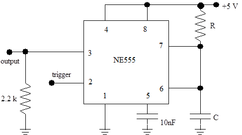 |
| Figure 11.3 Using NE555 in the single-pulse monostable mode |
Pick R and C such that the pulse duration is 1 second (see data sheets), and verify the proper operation of the circuit. Note: it is very important that the capacitor C must not be an electrolytic capacitor; choose its value accordingly! Explain how the circuit works, clearly indicating the manner in which you trigger it.
The 555 can also be used to generate frequency-modulated signals or pulse-width modulated signals (see data sheets). Feel free to experiment!
Some Applications
Problem D2.3
Design and build a digital frequency meter. The input signal is a 0 to 5V square wave from the function generator and is connected to the 7490s via a gate; the gate is opened for exactly one second using the 555 in its monostable mode. One push button is used to start the 555; one second later the frequency is displayed. Another push button resets the display. (This circuit can also be designed with one switch to do both functions.) The 7490s are read out via the 7-segment displays. Test your frequency meter by setting the function generator to frequencies between a few Hz and 100 Hz.
Problem D2.4
Modify the previous circuit, with some simple changes, into a two-digit digital stopwatch. It’s supposed to work like the real thing: there are two push buttons; pushing the first button once starts it, pushing it a second time stops it. The other push button resets it. Remember that the push buttons bounce. However, since they have only one contact instead of alternating between two, the “classical” de-bouncing scheme using a flip-flop cannot be applied. Hint: one solution uses a 555 in its monostable mode. Use the function generator to generate a 1 Hz or 0.1 Hz clock. You may need one additional 7490.
The conversion of voltage levels into digital numbers is important in the interface between digital processors (computers, transmission lines, etc.) and the real world. The integrated circuit ADC0804 (pin layout is in Figure 12.1 and data sheet is in the Appendix) contains a complete 8-bit analog-to-digital converter and the necessary circuitry to interface it to a microprocessor. Details about the operation can be obtained from the data sheets following this section. The ADC0804 is based on the successive-approximation principle (see, for example, Horowitz and Hill, p. 622). The following connections are available (also see list below).
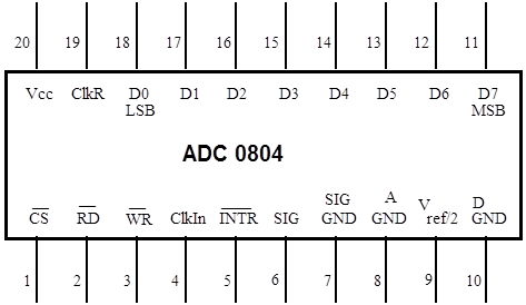
Figure 12.1 Pin assignment of ADC 0804 chip
Description of 20-pin-DIP ADC0804 chip
Pin 1 ![]() (chip select): It activates the ADC when a ‘0’ is at this input. The ADC will not accept read/write commands unless the chip is selected. This is very important when the ADC is connected to a computer data bus with many other devices (memory, other ADCs, DACs, I/O support, etc.).
(chip select): It activates the ADC when a ‘0’ is at this input. The ADC will not accept read/write commands unless the chip is selected. This is very important when the ADC is connected to a computer data bus with many other devices (memory, other ADCs, DACs, I/O support, etc.).
Pin 2 ![]() : A ‘0’ at this input will cause the (digital) result to be applied to the output pins if the chip is selected.
: A ‘0’ at this input will cause the (digital) result to be applied to the output pins if the chip is selected.
Pin 3 ![]() : A ‘0’ at this input will start the conversion process if the chip is selected.
: A ‘0’ at this input will start the conversion process if the chip is selected.
Pin 4 ClkIn: input of the clock generator trigger circuit. It can be used for an external clock signal.
Pin 5 ![]() : a ‘0’ at this output signals the end of a conversion process.
: a ‘0’ at this output signals the end of a conversion process.
Pins 6 & 7 Differential inputs. The voltage difference between these inputs is converted into an 8-bit number.
Pin 8 ADC ground.
Pin 9 Reference voltage. It determines the coefficient between the analog input and the digital output. The maximum digital output, 28 – 1, corresponds to twice the voltage of this pin.
Pin 10 Separate ground for the clock generator.
Pins 11-18 Digital outputs such that pin 11 corresponds to MSB (Most Significant Bit = 27) and pin 18 is LSB (Least Significant Bit = 20).
Pin 19 ClkR: output of the clock generator trigger circuit. Feedback of the trigger output to the input via an RC circuit causes the clock generator to oscillate.
Pin 20 VCC : positive supply voltage (+5 V).
Normally, the ADC is interfaced to a microprocessor (µp) or computer as shown in Figure 12.2.
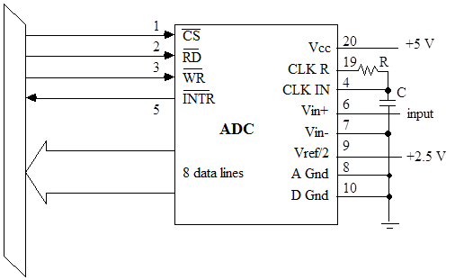
Figure 12.2 Connection of ADC0804 to a computer bus
The µp selects the ADC by asserting![]() , and sends a
, and sends a ![]() signal to start a conversion and then goes off to do something useful. After the ADC is finished with the conversion, it sends an interrupt (
signal to start a conversion and then goes off to do something useful. After the ADC is finished with the conversion, it sends an interrupt (![]() ) get the µp’s attention. Once the µp is ready to use the digitized output, it selects the ADC (
) get the µp’s attention. Once the µp is ready to use the digitized output, it selects the ADC (![]() ) and sends a
) and sends a![]() signal to cause the result to be applied to the outputs at pins 11 to 18, which are connected to the data bus. The outputs are so-called tri-state outputs (‘0’- ‘1’ - ‘inactive’) which in their inactive mode (
signal to cause the result to be applied to the outputs at pins 11 to 18, which are connected to the data bus. The outputs are so-called tri-state outputs (‘0’- ‘1’ - ‘inactive’) which in their inactive mode (![]() =‘1’) they don’t influence the data bus. The latter feature allows the outputs to be connected directly to the bus; without the
=‘1’) they don’t influence the data bus. The latter feature allows the outputs to be connected directly to the bus; without the ![]() =‘0’ signal, they don’t interfere with the normal operation of the bus.
=‘0’ signal, they don’t interfere with the normal operation of the bus.
Since we do not want to bother with a µp, we operate the ADC in a simplified mode: the ![]() input is connected to the
input is connected to the ![]() output and
output and ![]() is connected to ‘0’. As a result, when the ADC is done with one conversion, it sets the digital outputs and starts the next conversion. Strictly speaking, one has to provide a way to start the first conversion after power-up; usually, transients due to the power-up will take care of this.
is connected to ‘0’. As a result, when the ADC is done with one conversion, it sets the digital outputs and starts the next conversion. Strictly speaking, one has to provide a way to start the first conversion after power-up; usually, transients due to the power-up will take care of this.
Note: If your circuit is not working, it may be that the first conversion has not started. Look at ![]() on the scope. There should be many small, quick spikes appearing on it. If not, you must signal the first conversion. To do this, momentarily short
on the scope. There should be many small, quick spikes appearing on it. If not, you must signal the first conversion. To do this, momentarily short ![]() to ground with a second wire.
to ground with a second wire.
Problem D2.5 - Digital Voltmeter
We can use the ADC to build a simple 2-digit DVM (Figure 12.3). Use the 25k potentiometer and a DC input signal between 0 and 5 V.
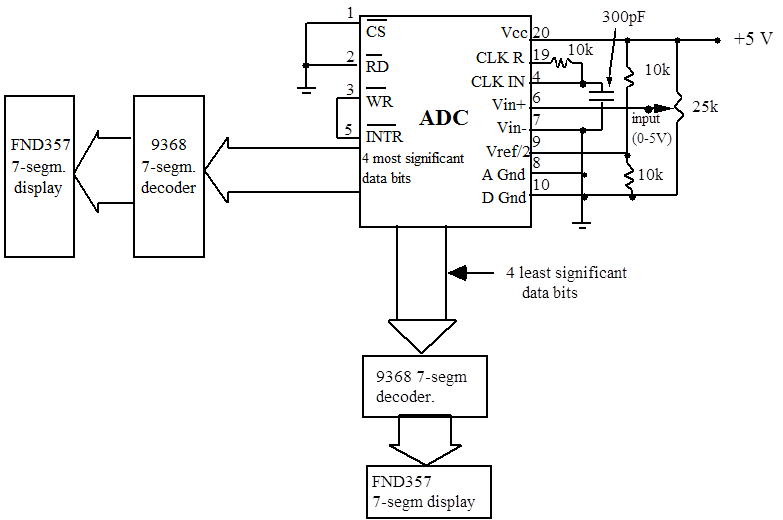
Figure 12.3 Circuit of a 2-digit DVM
Note that the display is hexadecimal; it shows 1,2,3...8,9,A,B,C,D,E,F.
Measure the clock frequency by examining the signal at pin 19. We advise that you use a frequency-compensated probe (a “10x probe”); the ordinary scope probe will disturb your measurement since the cable capacitance will alter the clock’s capacitance. Measure the conversion time by connecting the scope to pin 5. Does the conversion time depend on the size of the input signal? Do you expect it to, given that the ADC is based on the successive-approximation principle? How many clock cycles does a conversion take? See data sheets for more information.
Problem D2.6
Determine precisely the input voltages corresponding to steps of 10hex in the digital output, and plot the result. Is the ADC linear? From the data, calculate the conversion coefficient (counts/Volt). Does it agree with your expectations?
DAC and digital transmission
The currents from the analog outputs (pins 2 and 4) of the DAC08 (See Figure 12.4) correspond to the digital input number (pin 5 = MSB to pin 12 = LSB), with a conversion coefficient determined by the currents applied to the reference inputs (pins 14 and 15). Whenever the digital input is changed, the output settles to the new analog value within 100 ns. The DAC has two outputs (pins 4 and 2), a normal and an inverting one, which usually drive a differential amplifier. (See below, Section 12.3)
Problem D2.7
We are now ready to simulate a digital transmission chain, for example, used in modern phone systems or (with intermediate digital storage) in compact disc players. Build the circuit in Figure 12.4 (use ±12V) and connect the digital outputs of the ADC to the inputs of the DAC and connect the scope to the DAC outputs. Connect Vout– to Y input on the scope, invert it, and Vout+ to X input. Generate a 100 Hz, 1Vp-p sine wave oscillating between about +2 and +3 V and apply it to the ADC input; you will need to use a DC level shifter. Readjust the offset and the amplitude of the signal generator such that the DAC output signal does not clip. Try different input signal shapes and frequencies and sketch how the DAC output tracks the ADC input.
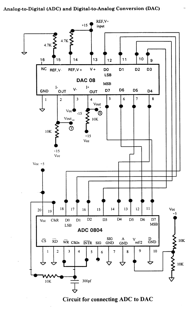
Figure 12.4
Problem D2.8
Shannon’s sampling theorem for minimal reproduction of a signal requires a sampling rate corresponding to twice the highest input frequency. This rate is often called the Nyquist frequency. Study this situation with your ADC/DAC system. What happens if the input signal is increased beyond half the sampling rate? Particularly interesting are the cases where the input frequency is close to a multiple of the sampling rate.
Problem D2.9
In practical applications, one usually wants to get rid of the steps in the output signal. This can be achieved by a low-pass filter to smooth the DAC output. Build the active filter circuit with an operational amplifier LF356 as shown in Figure 12.5 and measure its frequency response with sine waves. (Use the 10X scope probe.)
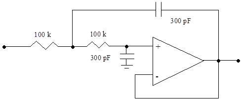
Figure 12.5 Active filter for smoothing the DAC output (use a LF356 Op Amp)
Connect the filter to the DAC output and observe its effect. Measure the frequency response of the ADC/DAC/filter transmission chain by measuring the output voltage with the scope. Try again to increase the input frequency well above the sampling frequency – at certain frequencies, you will still observe significant output signals at a lower frequency than the input frequency. This is called “ghosting”. To avoid this effect, real digital transmission systems have low-pass filters both in the inputs and outputs.
OPTIONAL: How about designing your own ADC? With your knowledge in analog and digital electronics, is shouldn't be too hard to build a 4-bit ADC. Start out with a homemade 4-bit DAC. The DAC resistors, if they are not too small, can be driven directly by any TTL output. Hook the DAC up to a 7490 counter driven by a gated clock signal (made using the 555), and add an op amp to compare DAC output and analog input. Now you need only a little logic circuit to stop the counter when the DAC output exceeds the input signal. Hint: switching transients from the DAC may be a problem – if necessary, add an appropriate RC low-pass filter at the DAC output. See the following diagram:
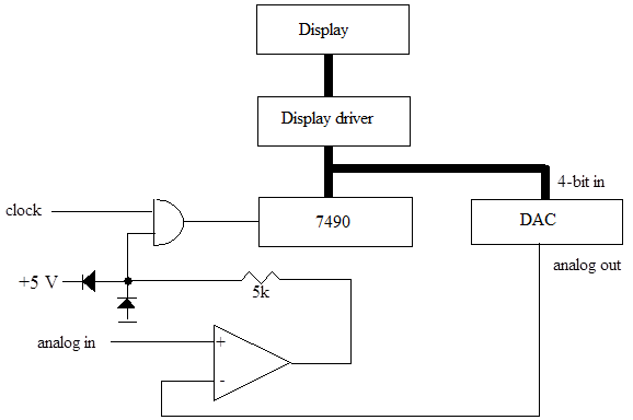
Figure 12.6 A simple ADC circuit
Note that the op amp is running at full open-loop gain and is used as a voltage comparator. The resistor-diode combination in its output limits the signal driving the gate. TTL gates don’t like 12 V input signals.
Questions
Problem D2.10
(See Section 12.5) Calculate the transfer function of the active filter as a function of the component values R and C.
Student Evaluation of Lab Report
After completeing the lab write up but before turning the lab report in, please fill out the Student Evaluation of the Lab Report.