Lab 7 - Op Amps II
University of California at Berkeley
Donald A. Glaser Physics 111A
Instrumentation Laboratory
Lab 7
Op Amps II
©2016 Copyrighted by the Regents of the University of California. All rights reserved.
Microelectronics Circuits, Sedra & Smith Chapter 2, skim Chapter 10
Art of Electronics Student Manual, Hayes & Horowitz Chapter 4 (Student Edition Book)
The Art of Electronics, Horowitz & Hill Chapter 4
Physics 111-Lab Library Reference Site
Reprints and other information can be found on the Physics 111 Library Site.
In this week’s lab you will continue your study of ideal op amp circuits. Circuits to be constructed include a current to voltage converter, a NIC (negative impedance converter), a gyrator, and an oscillator. The lab ends with the construction of a complex circuit that calculates root mean squares.
NOTE: You can check out and keep the portable breadboards, VB-106 or VB-108, from the 111-Lab for yourself ( Only one each please)
Before coming to class complete this list of tasks:
· Completely read the Lab Write-up
· Answer the pre-lab questions utilizing the references and the write-up
· Plan out how to perform Lab tasks.
All parts spec sheets are located on the Physics 111 Library site.
Pre-lab
1. How does a NIC work?
2. Derive the oscillator frequency of the circuit in 7.3. Draw the two output signals.
3. How does the logarithmic converter in 7.6 work?
4. How does the exponentiator in 7.8 work?
The Laboratory Staff will not help debug any circuit whose power supplies have not been properly decoupled!
Background
Almost all the circuits in this lab can be analyzed with the op amp golden rules.
Oscillators
Oscillators are circuits designed to put out periodic waveforms like sine or square waves. For example, oscillators are at the heart of our waveform generator, form a basic part of any radio or TV tuner, and generate the 3 GHz or so clock signals that characterize and control all computer CPUs.
(You might wonder why an oscillator is necessary in a tuner. It turns out that it is difficult to build sharp, variable-frequency bandpass filters, but is easy to build variable frequency oscillators. To exploit this difference, tuners use a complicated circuit called a superheterodyne receiver. Superheterodyne receivers use a tunable bandpass filter stage to crudely select the desired station, followed by a stage that mixes (multiplies) the signal with a signal from a variable frequency oscillator. As the receiver’s tuning knob is adjusted, the oscillator frequency shifts so that its beat frequency with the desired station is always at the same frequency: usually 455kHz for AM, and 10.7MHz for FM. The beat signal is then passed to a sharply tuned, single frequency filter, which rejects all but the desired station.
The oscillators in tuners are responsible for the ban on operating radio receivers during airplane takeoffs and landings. The FAA is afraid that the oscillator might accidentally broadcast a signal that would interfere with the cockpit instruments. Computers, CD players, gameboys, etc. are banned because of their clock oscillators. The ban is probably based more on paranoia than reality, and the FAA is slowly allowing more devices to be operated.)
You may have already encountered accidental parasitic oscillations. Many types of deliberate oscillator circuits exist, but the simplest is called a relaxation oscillator. The term relaxation oscillator dates from when these circuits were built with neon bulbs. A capacitor would be charged until it reached the neon bulb’s turn-on, or breakdown voltage. The bulb would then avalanche or relax down to its much lower turn-off voltage, discharging the capacitor, after which the process repeats. In this lab you will build a relaxation oscillator with an op amp. In practice, relaxation oscillators are usually built with special purpose chips like a 555.
Filters
Filter design is one of the most complicated subjects in analog circuit design; the UCB libraries, for example, have about twenty entire books solely on this subject. The ideal filter is called a brickwall filter; it has exactly unity gain in its pass region, exactly zero gain everywhere else, and does not induce any phase shifts. Unfortunately perfect analog brickwall filters are impossible to construct. Brickwall filters can be constructed digitally at the expense of a long time delay between the input and output signals. This delay allows a digital filter to use information from future times to calculate the response at the current time. Analog filters, however, must be causal; as they cannot anticipate the future, their response can only depend on past information, and they can never be perfect.
Many different filter designs exist, each attempting to optimize different aspects of filter performance. For example, the simple RC low and high pass filters you constructed at the beginning of this course, and other filters constructed entirely from passive components, suffer from gradual frequency response, unwanted phase shifts, and high output impedance. Better filters can be constructed with op amps. The Chebyshev active filter constructed in this lab is optimized for a sharp fall in its transition, or skirt region.
In the lab
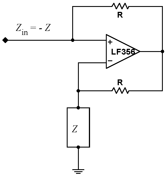
Problem 7.1 - Negative Impedance Converter (NIC)
| A generic NIC, shown at right, is a negative impedance converter. Looking into Vin, the NIC appears to have an impedance -Z to ground. In other words, the circuit inverts it internal impedance Z to -Z. |
|
|
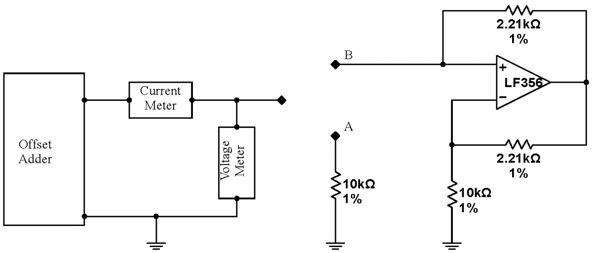
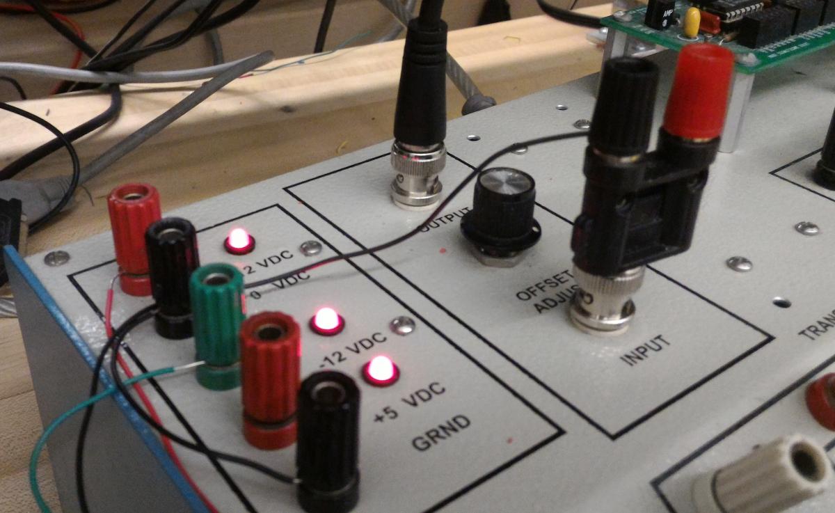
Construct the circuit below. Use matched, 1%, precision resistors. To match resistors, start with ten to twenty of each value. Measure the resistance of each resistor, and select the two that have the closest values. Note that the offset adder needs to be explicitly grounded. One way to do this is illustrated in the photo at right. The offset adder input is not otherwise used in this problem. Begin investigating this circuit by connecting the meters to point A. Vary the offset adder voltage, and prove that the $10\,\mathrm{k}\Omega$ resistor does indeed behave appropriately. (This purpose of this step is to check your meter polarities.) Next connect the meters to point B. Vary the offset adder voltage and measure the current. Prove that the NIC appears to be a $-10\,\mathrm{k}\Omega$ resistor. |
 |
 |
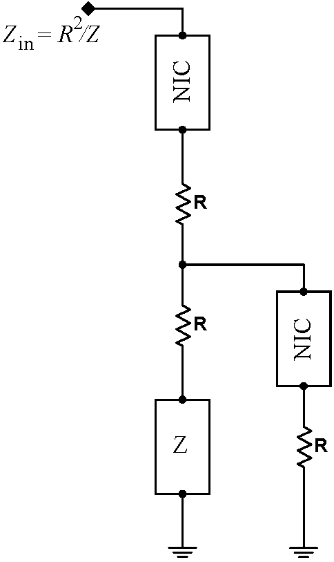
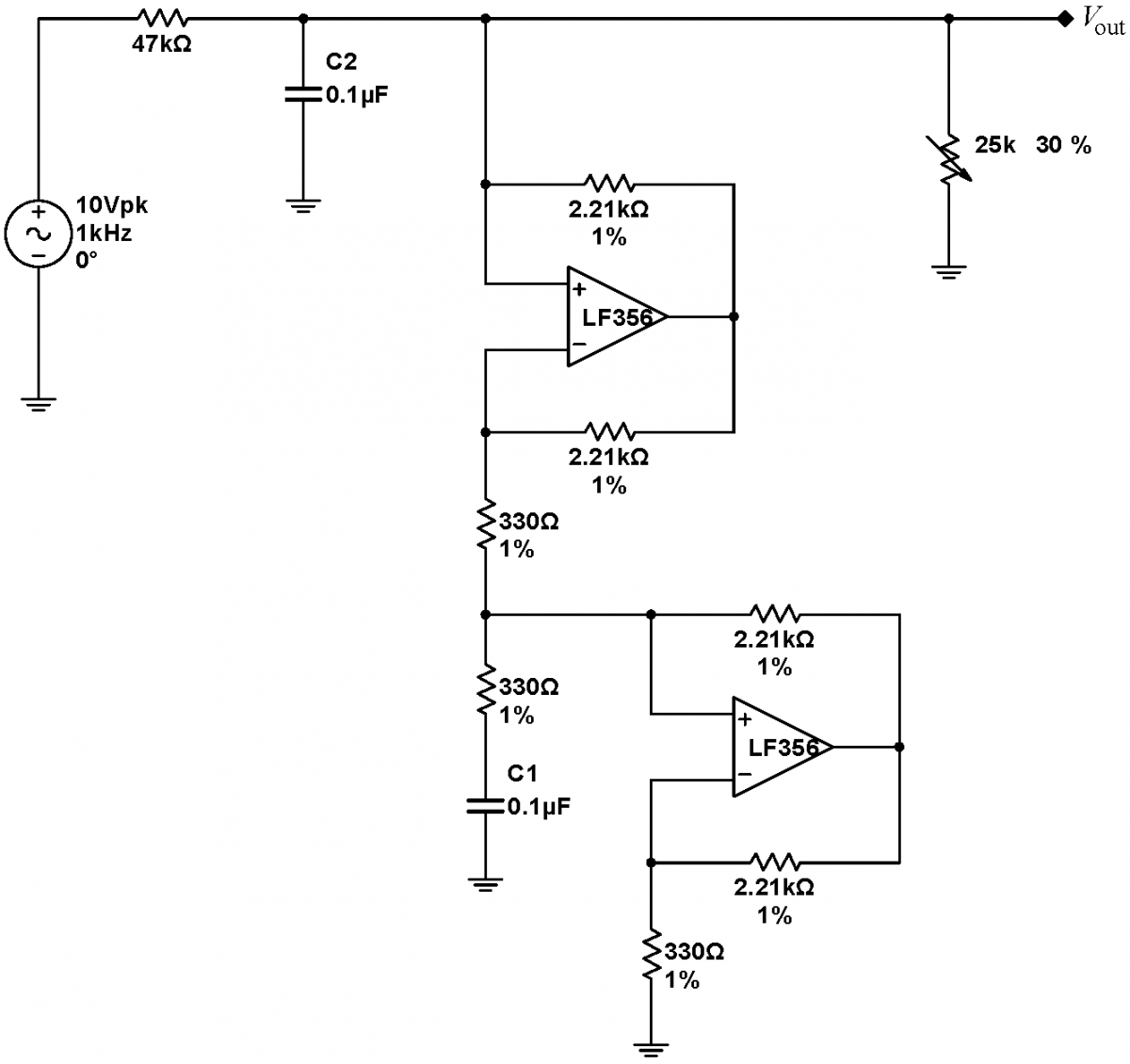
Problem 7.2 - Gyrator
|
A gyrator is a circuit that converts an impedance $Z$ to $R^2/Z$ . Gyrators can be synthesized from two NICs as show in the block diagram at right. The components directly below each individual NIC form the impedance $Z$ of that particular NIC. When the explicit Z in the gyrator comes from a capacitor, to $Z=1/j\omega C$, and the gyrator will look like it has an impedance $j\omega CR^2$; i.e. it will look like an inductor of inductance $CR^2$. As high quality inductors are difficult to obtain, bulky, and nearly impossible to fabricate on integrated circuits, inductors are often replaced with gyrators, particularly in filters and resonant circuits. |
 |
|
Construct the resonant (fake $L$)$C$ circuit below. Use matched 1% precision resistors: all three $330\,\Omega$ resistors must match, but the pair of $2.21\,\mathrm{k}\Omega$ resistors in the top NIC need not match the pair of $2.21\,\mathrm{k}\Omega$ resistors in the bottom NIC. This is one of the most touchy circuits that you will build this semester; the better matched the resistors, the better the circuit will work. Note that 47k resistor is used to isolate the wavefunction generator from the rest of the circuit. Drive the circuit with a sine wave in the neighborhood of $5\,\mathrm{kHz}$. What is the circuit’s resonant frequency? What is its calculated resonant frequency? Adjust the variable resistor to maximize the $Q$. This circuit tends to oscillate spontaneously. These spontaneous and unwanted oscillations can be differentiated from the desired response to the signal generator by phase locking the oscilloscope to the signal generator and displaying the generator output on the screen. If the output of the circuit is locked and has a constant phase relationship to the generator, the circuit is behaving properly; if the output is not phase locked, the circuit is oscillating spontaneously.
The oscillations can be killed by decreasing the resistance of the variable resistor, but this will also lower the $Q$. The system exhibits substantial hysteresis. Once you lower the resistance to kill the oscillations, you can typically turn the resistance back up significantly without the circuit rebreaking out into oscillations. Turning the circuit power on and off, and grounding the output, can also either kill or initiate the spontaneous oscillations.
Now change the drive to a 10Hz, high amplitude square wave, and watch the circuit ring. What is the $Q$ calculated from the number of rings?
Change the $0.1\,\mu\mathrm{F}$ capacitor C1 in the RLC circuit to a $1\,\mu\mathrm{F}$ capacitor. Does the resonant frequency change appropriately? |
 |
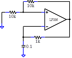
Problem 7.3 - Relaxation Oscillator
|
Build the relaxation oscillator at right. Save images of the signal at both the op amp output and across the capacitor. How does the circuit work? (Hint‑Think about the hysteretic comparator circuit.) What is the oscillator’s output frequency? How does it compare to theory? |
 |
 Problem 7.4 - Filters
In Labs 1 and 2, you constructed several filters. However, simple, single stage RC filters like most of the ones you constructed in the earlier labs, are often inadequate. For instance, you might need a low pass filter that rejects signals above its passband more strongly than you can get with a single stage filter. You can obtain a sharper cutoff with a multistage filter; a filter that cascades several single stage filters. Or, you might want to build a bandpass filter, which is inherently a multistage filter. One problem with building multistage passive filters, like the bandpass filter in Lab 1, is that the second stage loads the first stage. Consequently, the performance of the first stage is not what you would calculate for an isolated first stage, and often the circuit does not perform well.
This multistage loading problem can be easily fixed by building an active filter. So far, the filters that you have built have been passive filters; a passive filter is a filter made from only resistors, capacitors and inductors. Active filters often perform much better than passive filters; an active filter contains an amplifying element like an op amp.
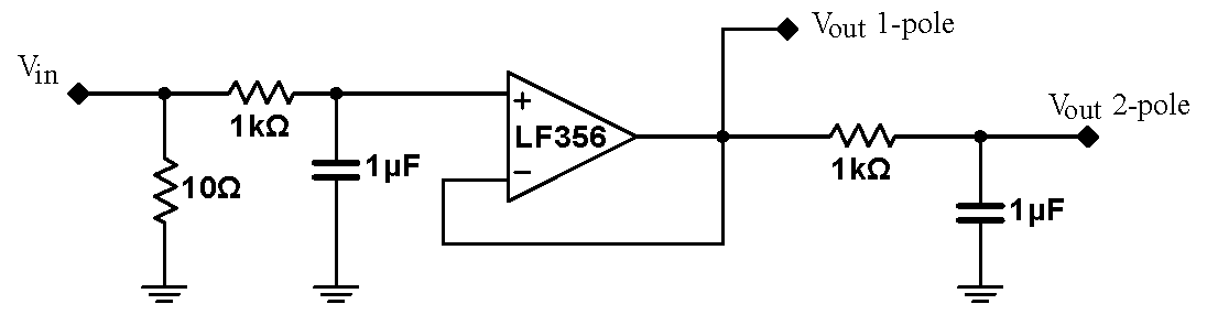
|
An easy way to decouple the stages in a multistage filter is to use a follower. Build the circuit at right. It consists of an initial $RC$ filter, a follower, and an identical $RC$filter. The circuit has two outputs: one, which gives the signal after only the first $RC$filter, and the second which includes both $RC$ filters. Feed the outputs into channels 2 and 3 on your scope. (Send the input signal into channel 1.) Set up auxiliary triggering. Casually explore the behavior of this circuit near its $3\,\mathrm{dB}$ frequency of about $160\,\mathrm{Hz}$. You should observe that above the passband, the 2-pole output is more strongly attenuated than the 1-pole output. (Multistage filters are more commonly called multi pole filters. This terminology comes from the complex analysis of the filter response; every stage will contribute a pole in the complex plane.) Note that the $10\,\Omega$ resistor reduces the effects of the changing input impedance of the filter, but does not otherwise affect the performance of the filter. Do not disassemble your circuit, it will be used again in this exercise. |
 |
|
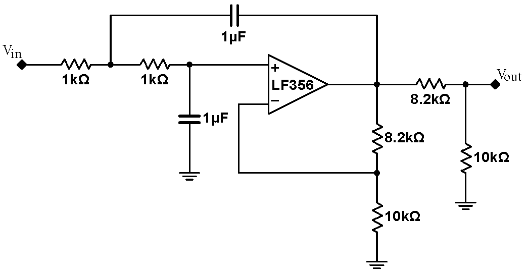
With a more sophisticated topology, it is possible to construct a filter with a sharper cutoff than the two stage $RC$ filter above. Construct the 2-pole Chebyshev Sallen-Key filter at right. (Sallen-Key refers to the topology of the components. Chebyshev refers to the the particular optimization used to select the values of the components; there are several common optimizations, all having somewhat different properties.) Feed the output of this circuit to channel 4 on your scope. Drive the input of this filter with the same input that you are using to drive the RC filter; you should be able to see all four output traces on the screen at the same time. Casually explore the behavior of this circuit near its $3\,\mathrm{dB}$ frequency, which should also be near $160\,\mathrm{Hz}$. |
 |
|
Filters, as well as many other circuits, are frequency dependent, and it can be painfully slow to explore their behavior. The signal generator has a frequency sweep mode that can greatly speed up such measurements. Normally, the signal generator outputs a single frequency. In sweep mode, the signal generator scans through a preset range of frequencies. Watch the video at right to understand how to set up a frequency sweep. |
|
Setup your signal generator to scan from $20\,\mathrm{Hz}$ to $1\,\mathrm{kHz}$, using a sweep time of $2\,\mathrm{s}$, a return time of $0\,\mathrm{s}$, and a log scan. The amplitude of your scan should be $6\,\mathrm{Vpp}$. Set your scope to display channels 2, 3 and 4, (1-pole RC, 2-pole RC, Chebyshev), and use a horizontal scan of $200\,\mathrm{ms}/\mathrm{div}$. You should see traces like those at right. Notice:
|
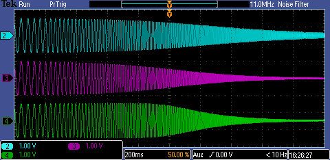 |
|
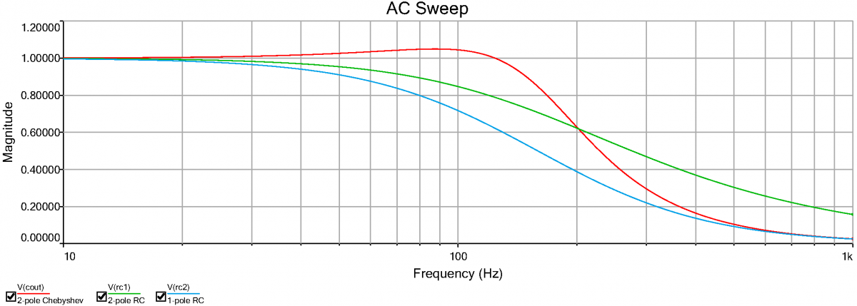
From the frequency response curves, you might conclude that the Chebyshev filter, having the steepest skirt, is always the best filter. However, the Chebyshev filter has some imperfections. For instance, as shown in the spice simulation at right, the Chebyshev filter has a ripple in its passband; just before it begins to attenuate, the signal actually increases by about 5%. The $RC$ filters do not have a ripple. Measure the approximate size of the Chebyshev ripple. Since the ripple is small, this is difficult to do precisely. It may be easiest to accomplish by changing your signal generator to output a single frequency, and setup an amplitude measurement on the Chebyshev channel. Manually scan the signal generator frequency until you find the peak near $100\,\mathrm{Hz}$. Then use averaging to measure this peak. Also measure the signal at $10\,\mathrm{Hz}$ for comparison. Note that the size of the ripple depends on the actual values of the resistors and capacitors in your circuit, and may not agree precisely with computer simulations. Sometimes, these sorts of passband ripples are acceptable, and a Chebyshev filter (which will always have ripples) is acceptable. Other times, ripples are not acceptable, and you should use an $RC$ filter (which will never have a ripple), or another type of rippleless filter, like a Butterworth filter. |
 |
|
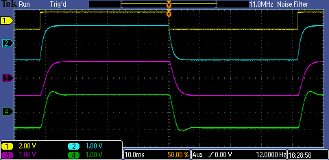
So far, we have only considered the frequency response of the filters. We should also consider the transient response of the filters, i.e. the response in time to an abrupt change to the input signal. Set your signal generator to output a $12\,\mathrm{Hz}$ square wave. Display the square wave on channel 1 of your scope. You should see traces like those at right. Notice that while the $RC$ filters asymptote to their final values smoothly, the Chebyshev filter overshoots. Measure the size of the overshoot. Sometimes, one wants to optimize a filter to most faithfully reproduce an input transient. Yet another type of common filter, a Bessel filter, does this best. All these filters [Butterworth, Chebyshev, Bessel (there are others)], as well as low pass, high pass, bandpass, and bandreject filters, can be built using the Sallen-Key typology by adjusting the component values and swapping the placement of the resistors and capacitors. |
 |
This lab culminates with the construction of an RMS converter, similar to the RMS converter found in the DMMs. The circuit calculates
$\displaystyle V_\mathrm{RMS}=\sqrt{\frac{1}{T}\int^T|F(t)|^2\,dt}$
The circuit is quite complicated, and involves ten op amps. Fortunately the circuit is quite modular, and each module can be tested individually. The functions performed by the modules are, in sequence: absolute value, square, time average, and square root. The square (and square root) modules consist of three sub modules: a logarithm, doubler (halfer) and exponentiator.
Build your circuits cleanly; neatness will pay off. Lay out the circuit from left to right. As you go along, make sure that you leave enough space for all ten op amps.
In all cases, use 1% resistors; when we don't stock the required value, synthesize it from parallel or series combinations of other resistors.
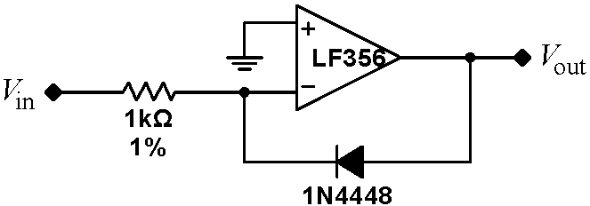
Problem 7.5 - Absolute Value
|
The first module in the RMS converter takes the absolute value of the signal. Construct the circuit at right. Drive the circuit with a variety of signals, amplitudes, and offsets from the waveform generator. Save some illustrative images. How well does the circuit work? Disassemble the second op amp and its $1\,\mathrm{k}\Omega$ feedback resistor in this module, leaving the first op amp and its associated feedback network in place for the RMS converter. |
 |
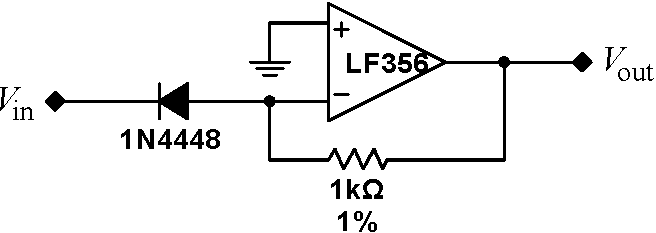
Problem 7.6 - Logarithm
|
Next, we need to square the signal after taking its absolute value. This operation is performed by taking the log of the signal, multiplying it by two, and then exponentiating. Build the circuit at right, which takes advantage of the exponential dependence of diode current on voltage, $\displaystyle i(V)\approx i_\mathrm{sat}\exp\left( \frac{eV}{nkT}\right)$ to take the logarithm of its input signal. As with all the remaining circuits, a good initial debugging signal is an offset triangular wave. Note that this circuit expects a negative signal; your signal generator can be easily set to make an entirely negative signal with the High Level and Low Level options on the Amplitude menu. Configure the signal generator to output a DC voltage by putting it on the More->More->DC setting. Drive the circuit with a series of DC input voltages, and record the input and output voltages at each point. Plot your data; how close is it to a true natural logarithm? Do you have to scale and offset the data to make it match a logarithm? |
|
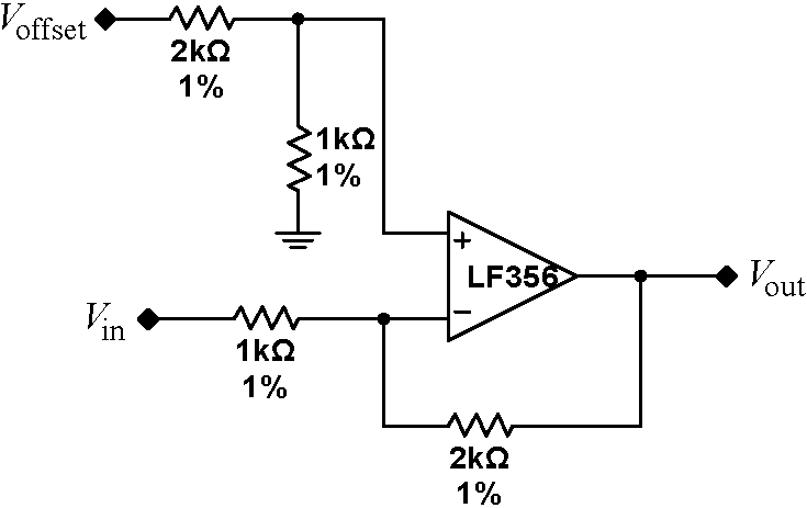
Problem 7.7 - Multiplier and Shifter
|
Build the circuit at right, which multiplies the logarithm of the initial signal by negative two. The circuit also offsets the signal by a constant $V_\mathrm{offset} $. In Exercise 7.6, you should have found that the signal needs to be scaled and offset. Adding in $V_\mathrm{offset} $ accomplishes these shifts such that the output of the squaring section of the RMS converter is equal, not merely proportional, to its input. Rather than trying to estimate the proper shift, we can use a circuit to calculate the proper value. It turns out that the proper value for the offset is whatever the circuit in 7.6 would output for a $-1\,\mathrm{V}$ input. |
 |
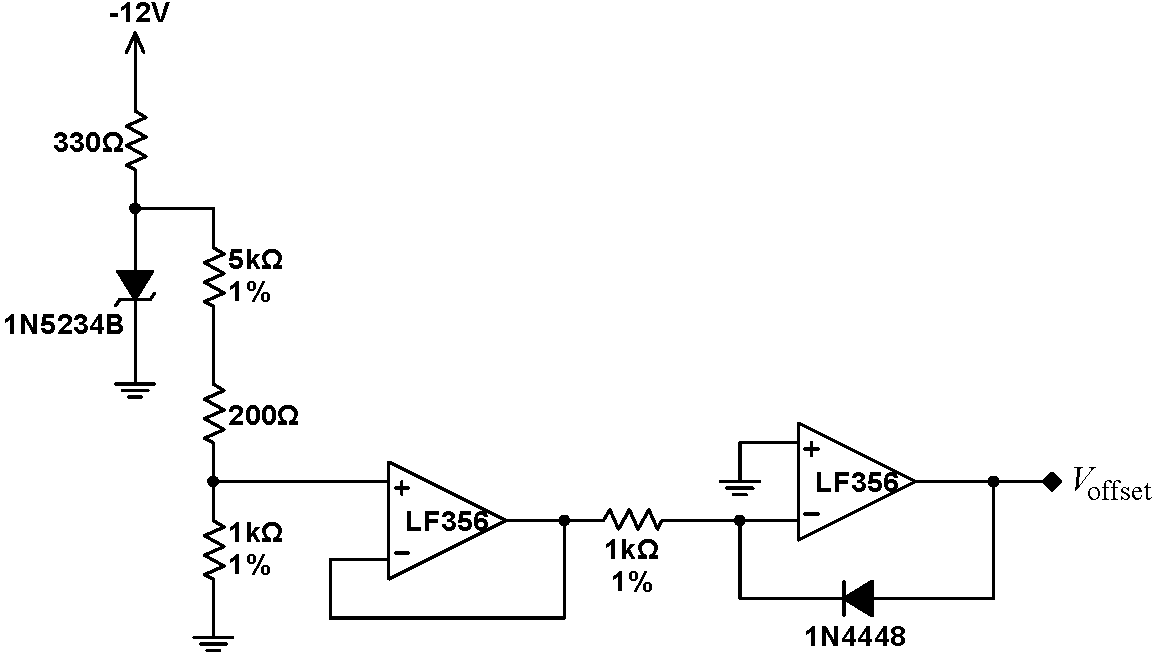
|
Build the circuit at right to calculate the offset. The $330\,\Omega$ and $200\,\Omega$ resistors are the only the resistors in the RMS converter that should not be 1% resistors. The voltage across the Zener diode is nominally $6.2\,\mathrm{V}$, however there will be some variation between Zeners, and this voltage will vary. The divider network which immediately follows should reduce the Zener voltage such that the output of the first op amp is $-1\,\mathrm{V}$; if it is not $-1\,\mathrm{V}$, adjust the value of the $200\,\Omega$ resistor to make it $-1\,\mathrm{V}$. You may have to change the location of this resistor to the bottom of the divider. You should find that the output of this circuit is approximately $+0.6\,\mathrm{V}$. Drive the multiplier with the log output, and check that it doubles and offsets its input. You do not need to record anything. Note that the Zener diode and the 1N4448 diodes are almost identical in appearance. Make sure that you keep track of which is which; you will become hopelessly confused if you swap them. |
 |
Problem 7.8 - Exponentiator
|
To exponentiate the signal, build the circuit below. Use an offset triangle wave to debug your circuit. (The circuit requires a negative input.) Then drive the circuit with a series of DC input voltages, and record the input and output voltage at each point. Plot your data; how close is it to a true exponential? |
 |
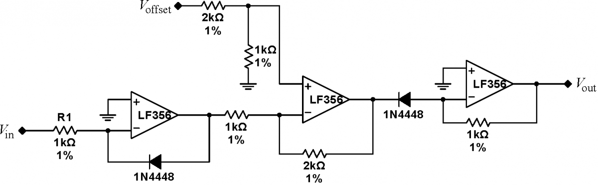
Problem 7.9 - Squarer
|
Finish the squaring module by hooking all the circuits together, as shown below. Drive the circuit with a series of DC input voltages, and record the input and output voltages at each point. Plot your data; how well does the module square its input signal? It should be accurate to better than $\pm10\%$. What is the largest input signal accepted by the module before it saturates? Remove the input resistor R1, but keep the rest of the circuit. |
 |
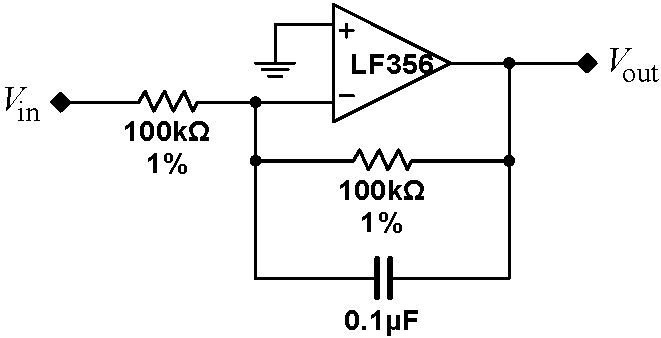
Problem 7.10 - Time Averager
The next step is to time average the signal. The time average of a signal $\left<H\right>$ is found by integrating:
$\displaystyle\left<H\right>=\frac{1}{T_f-T_i}\int_{T_i}^{T_f}H(t)\,dt$
If the signal is repetitive, the limits of integration are over one cycle. What if the signal is not repetitive or we do not know the repetition frequency? The integral
$\displaystyle\left<H\right>(t)=\frac{1}{\tau}\int_{-\infty}^{t}H(t^\prime)\exp\left(\frac{t^\prime-t}{\tau}\right)\,dt^\prime$ (1)
generalizes the averaging formula. This formula is easy to implement electronically. [Note: the circuit below also introduces a multiplicative factor of -1.]
|
Build the integrating averager at right. Drive the circuit with a variety of waveforms, and show that its output is the inverse average of its input. Over what frequency range does the circuit work? What sets this range? |
 |
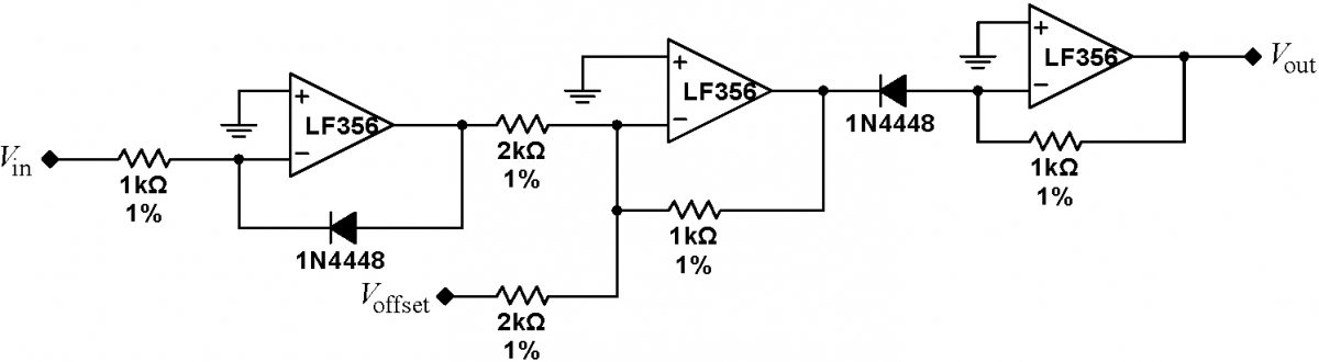
Problem 7.11 - Square Rooter
|
Finally, we need to take the square root of the averager signal. The required circuit is very similar to the squaring circuit. Build the circuit at right. Debug each section independently. Use the offset voltage from 7.7. Drive the circuit with a series of DC input voltages, and record the input and output voltage at each point. Plot your data; how well does the module take the square root of its input signal? |
 |
Problem 7.12 - RMS Converter: No Averaging
Connect all the modules. Your circuit should now be as below:
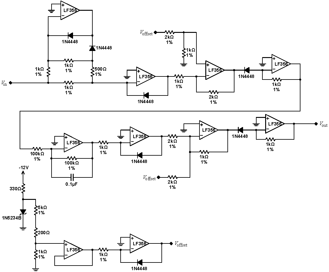
Temporarily disconnect the averaging capacitor. Use the waveform generator to drive the RMS converter. What output should you expect to see? Your signal will probably be off by a multiplicative constant. Fiddle with the values of the resistors in the time averager to obtain the (approximately) correct normalization.
Problem 7.13 - RMS Converter
Reconnect the averaging capacitor. What happens to the output? Use the circuit to determine the RMS value of its input for a variety of input signals. Compare the result with the reading from the DMM on the RMS setting, or with an RMS measurement on the scope. How well does your circuit work? Note that your circuit will be somewhat temperature dependent, and will drift from moment to moment.
The following problems can be done away from the lab.
Problem 7.14 - Gyrator Analysis
Analyze the gyrator block diagram, and prove that it behaves as claimed.
Problem 7.15 - Absolute Value Analysis
|
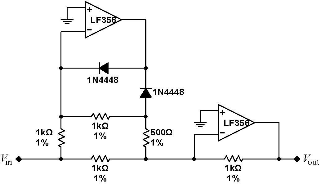
The behavior of the absolute value circuit is easiest to understand by considering negative and positive input signals separately. Begin by recalling that the Golden Rules insist that the $V_-$ inputs to both op amps are held at virtual grounds; this is true regardless of the sign of the input signal. With a negative input signal, we would expect the output of the first op amp to be positive. Then, the grayed out diode shown in the absolute value circuit at right is reversed biased and will carry no current; we will ignore it henceforth. How much current will be be carried by the $500\,\Omega$ resistor? What is the total current entering the $V_-$ node of the second op amp? What output voltage on the second op amp is required to carry this current away? |
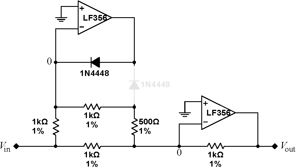 |
| Conversely, with a positive input signal, we would expect that the output of the first op amp will be negative. In this case, the other diode will be reversed biased, as shown at right, and can be ignored. What must be the voltage on the node labeled V such that there is a virtual ground on the $V_-$ input of the first op amp? In this case, what is the total current entering the $V_-$ node of the second op amp? What output voltage on the second op amp is required to carry this current away? | 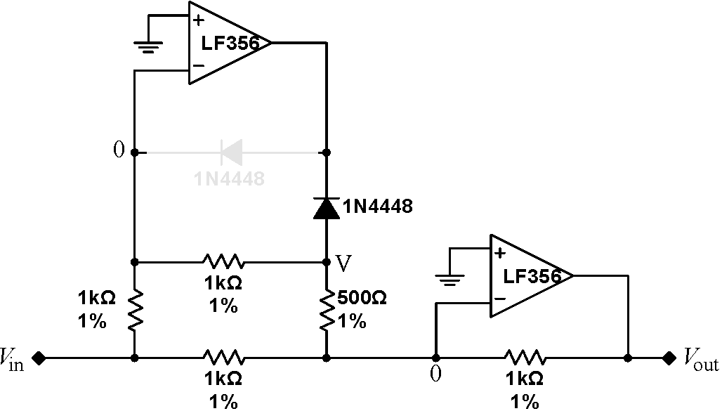 |
Problem 7.16 - Squarer Analysis
Show arithmetically that the circuit in 7.9 is a true squarer with no offsets or multiplicative factors.
Problem 7.17 - Averager Analysis
Derive the differential equation that describes the dynamics of the time averager circuit in 7.10. Show that Eq. (1) is a solution to that differential equation. What is τ?
Student Evaluation of Lab Report
After completing the lab write up but before turning the lab report in, please fill out the Student Evaluation of the Lab Report.