Lab 5 - JFET Circuits II
University of California at Berkeley
Donald A. Glaser Physics 111A
Instrumentation Laboratory
Lab 5
JFET Circuits II
©2016 by the Regents of the University of California. All rights reserved.
Art of Electronics Student Manual, Hayes & Horowitz Chapter 3
The Art of Electronics, Horowitz & Hill Chapter 3, 7.1.1-7.1.3
Physics 111-Lab Library Reference Site
Reprints and other information can be found on the Physics 111 Library Site.
Lab 3 Appendices: Data sheets and Curve Tracer operation.
NOTE: You can check out and keep the portable breadboards, VB-106 or VB-108, from the 111-Lab for yourself ( Only one each please)
In this lab you will investigate some more sophisticated JFET circuits, such as voltage amplifiers, differential amplifiers, attenuators, and modulators.
Before coming to class complete this list of tasks:
· Completely read the Lab Write-up
· Answer the pre-lab questions utilizing the references and the write-up
· Perform any circuit calculations use Matlab or anything that can be done outside of lab use RStudio (freeware).
· Plan out how to perform Lab tasks.
All part spec sheets are located here the Physics111 Library site
Pre-lab
1. Explain in detail how a signal applied to the gate of one transistor in a differential amplifier can produce an output on the drain of the other transistor.
2. What are parasitic oscillations? How do you minimize them?
Do not forward bias the JFET gates. Forward gate currents larger than 50mA will burn out the JFETs!
The Laboratory Staff will not help debug any circuit whose power supplies have not been properly decoupled!
Background
Voltage Amplifiers
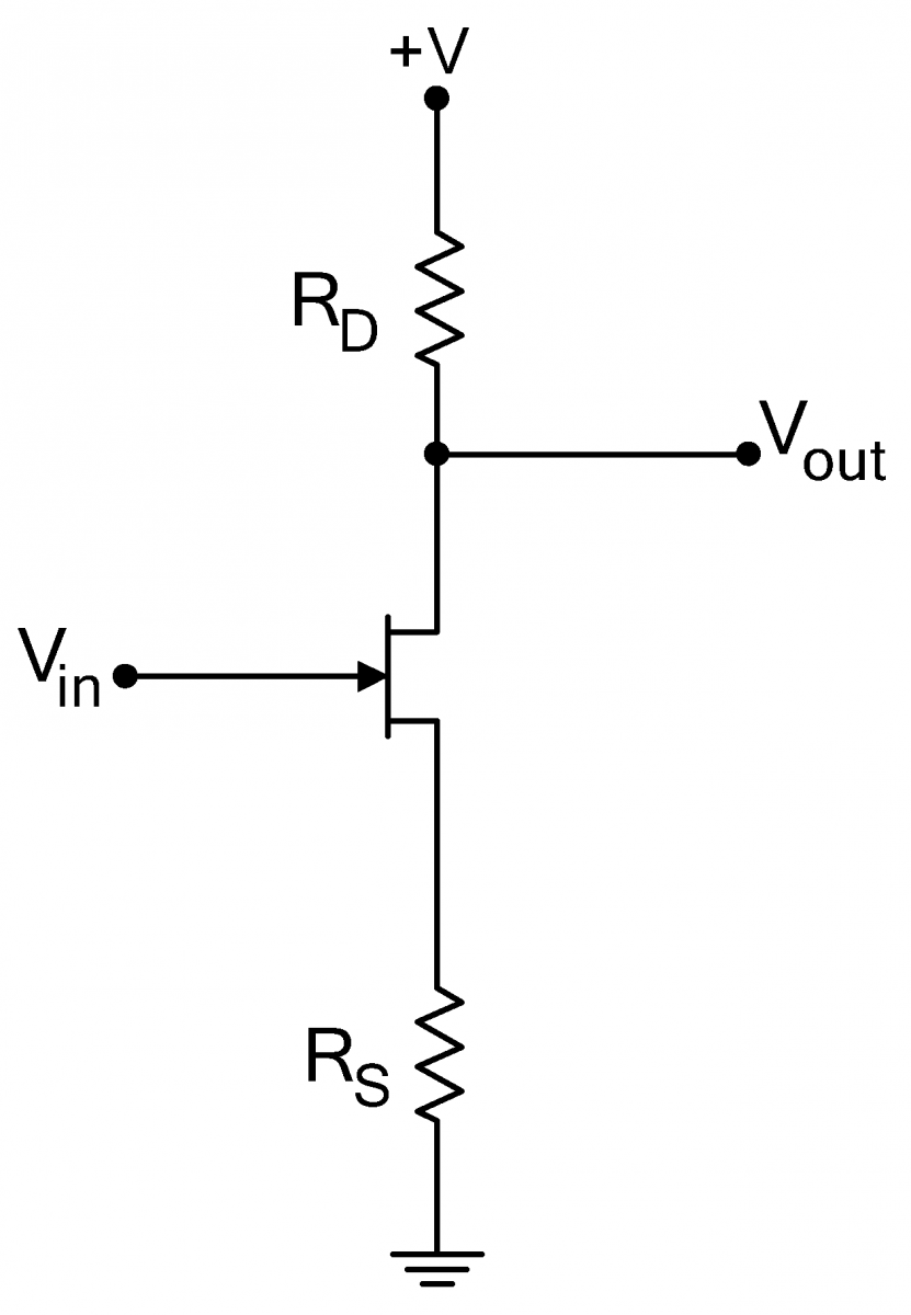
| Adding a drain resistor $R_D$ to a source-follower turns it into a voltage amplifier, as shown to the right. This topology amplifier is known as a common source amplifier
The equivalent small signal circuit for the amplifier is shown to the extreme righnt and is most easily understood by remembering that the current in a source follower is given by $\displaystyle i_s=\frac{v_{in}}{R_S+r_s}$. where $r_s=1/g_m$. Since this current is unchanged by the addition of the drain resistor, the output voltage will be $\displaystyle v_{out}=-R_Di_s=-\frac{R_D}{R_S+r_s}v_{in}$. Thus the gain of the amplifier is $G=-R_D/(R_S+r_s)\approx-R_D/R_S$, (1) where the last equality assumes that the transconductance is high.
|
 |
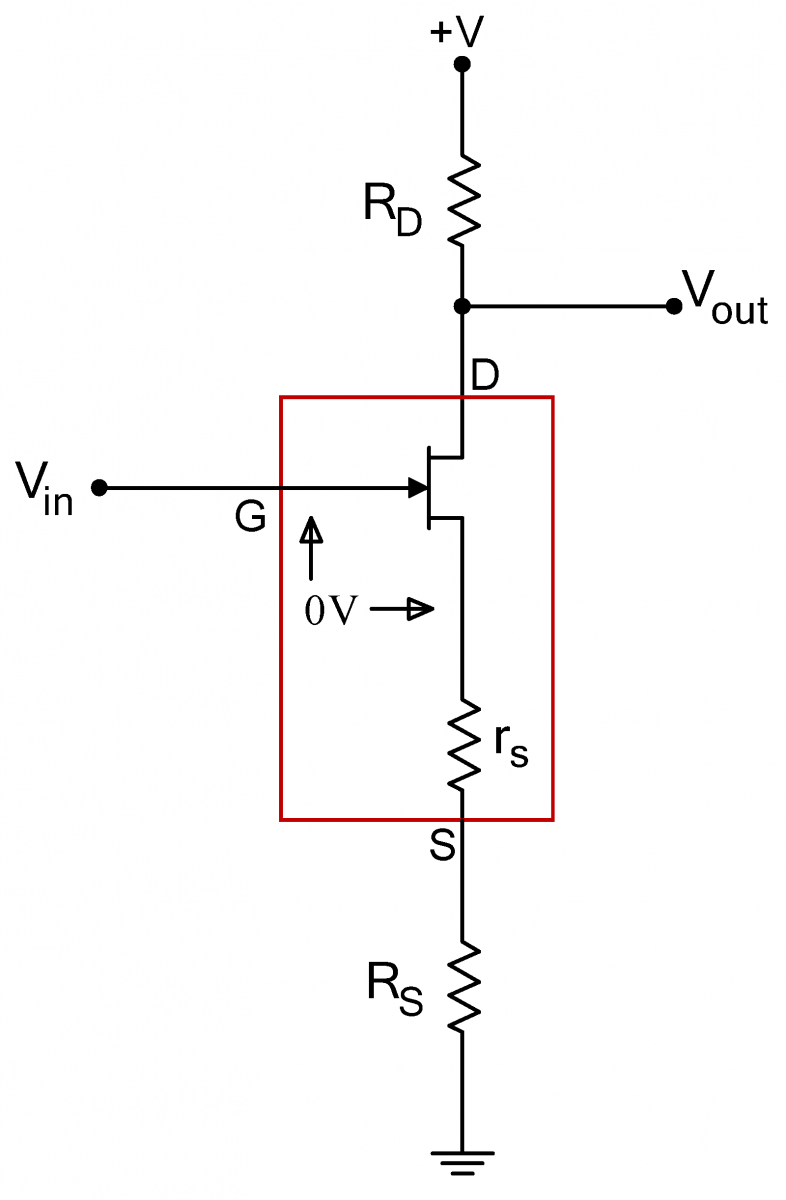 |
As with the source follower, the input current is given by the gate leakage current, so the amplifier’s input impedance is extremely high. The output impedance of the amplifier equals the drain resistance $R_D$, and unlike the output impedance in the follower circuit, it is not low.
Differential Amplifiers
|
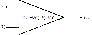
Differential amplifiers have two inputs, V+ and V-, and one or two outputs. In an ideal differential amplifier, the amp’s output depends solely on the difference between the two inputs, |
 |
Differential amplifiers are one of the most common building blocks in analog circuit design. The front end of every op amp, for example, consists of a differential amplifier. Differential amplifiers are used whenever a desired signal is the difference between two signals, particularly when this difference is masked by common mode noise.
Electrocardiograms are an example of the use of differential amplifiers. The heart generates electrical signals, which can be detected by electrodes placed against the skin, but the signal from a single electrode would be swamped by background pickup; as you know from touching the input to an oscilloscope, the body is an excellent antenna for noise in frequencies ranging from $60\,\mathrm{Hz}$ to $100\,\mathrm{MHz}$. Fortunately these undesired signals are nearly equal everywhere on the body. By using two pickups, placed so that the signal from the heart has the opposite sign on the pickups, and amplifying the difference between the two pickups with a differential amplifier, the desired signal from the heart can be preferentially amplified over the unwanted noise.
| Differential amplifiers are constructed from a matched pair of transistors as shown to the right. The two inputs are on the gates of the transistors. The drain of either transistor can be used as the output; in some cases both JFET drains are used to provide a differential output, i.e outputs of opposite phase. | 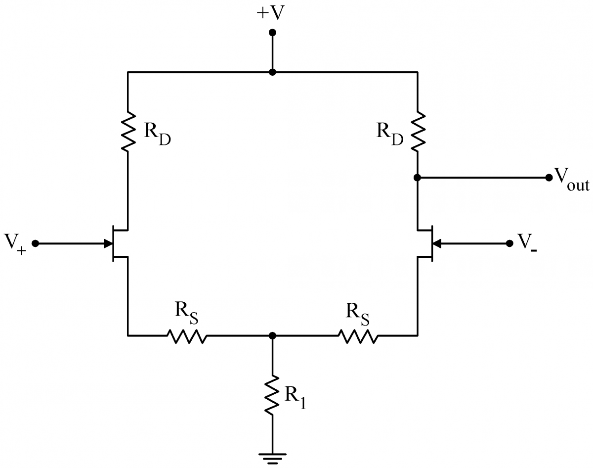 |
|
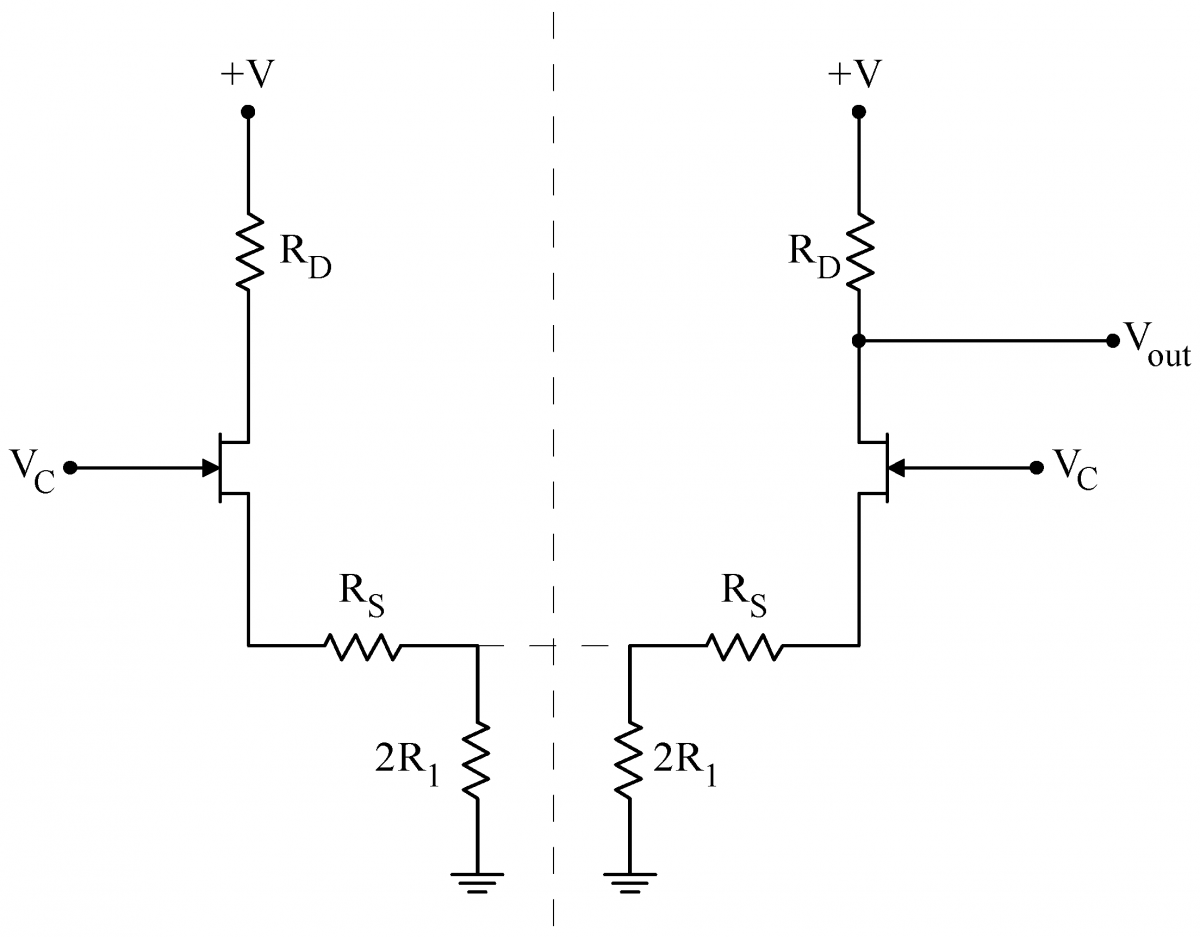
When driven with a common mode signal only, symmetry tells us that both sides of the circuit will behave identically. In this case, we can pretend to split the circuit down the middle, as shown at right. The two $2R_1$ resistors combine to make the original $R_1$. Symmetry requires that the two upper ends of the $2R_1$ resistors be at the same potential; thus no current would flow in the dashed line that connects the two ends. Since there is no current, we can pretend that the resistors are disconnected. We can use Eq. (1) to calculate the gain of the two halves of the circuit individually. This common mode gain is minus one times the following: In practice, the common resistor $R_1$ is always made much greater than the source resistors, so the gain reduces to . $R_D/2R_1$Further, $R_1$ is always chosen to be much larger than the drain resistor $R_D$. Consequently, the gain for common mode signals is low and these signals are strongly attenuated. |
 |
|
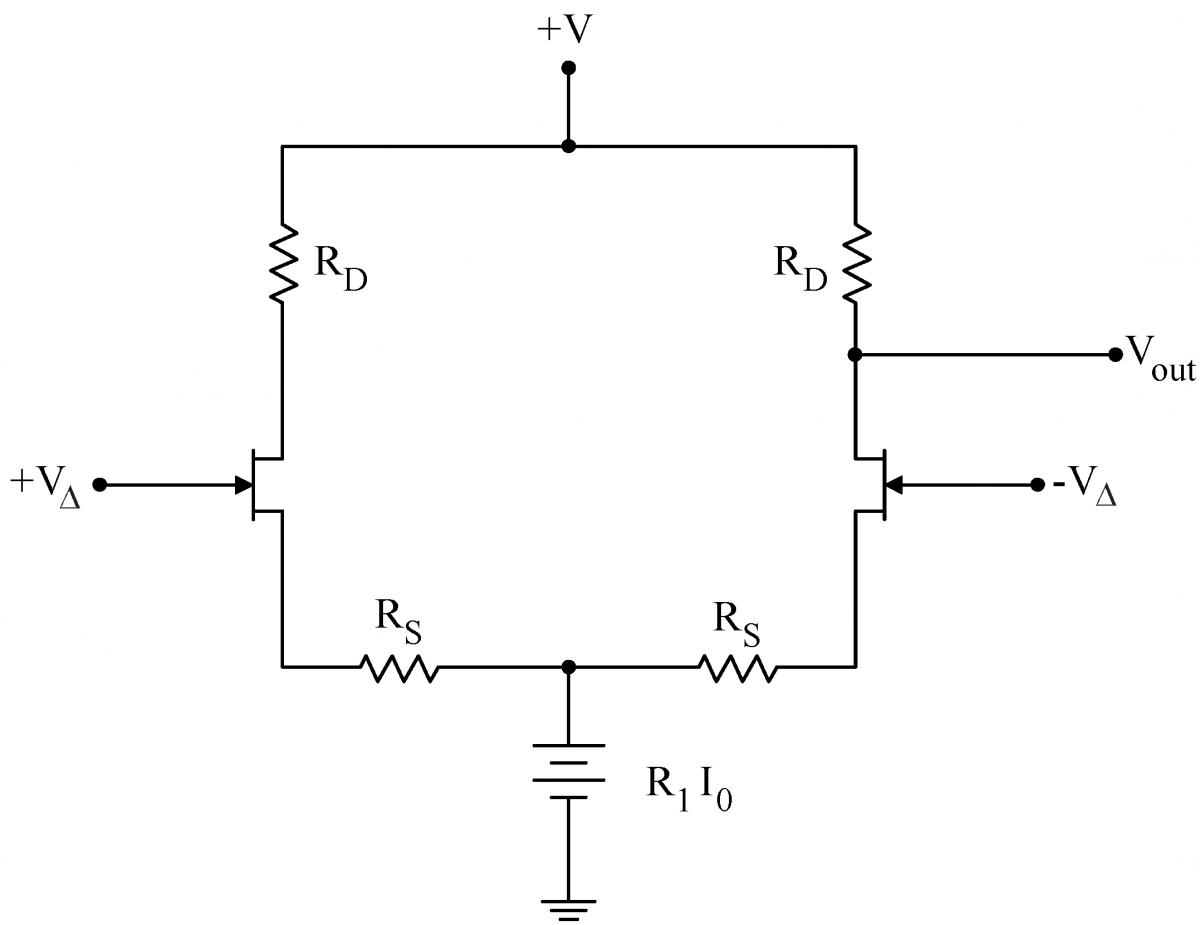
The response of the two transistors to a small differential signal $ V_\Delta$, on the other hand, will be equal and opposite. If the current through the left JFET increases ($V_+>0$), the current through the right JFET will decrease by an equal and opposite amount. The net current flow $I_0$ through, and voltage drop across, the common resistor will not change with $ V_\Delta$. Consequently the common resistor can be replaced with a conceptual voltage source of strength $R_1I_0$, as depicted at right. Since the two sides of the circuit are only connected at place held at constant voltage by the conceptual battery, the two sides effectively decouple. Then Eq. (1) yields the differential gain (two factors of -1 result in a +1 here) $\displaystyle \frac{R_D}{R_s +r_s}$ (3) If we choose the drain resistors, $R_D$, to be large compared to the source resistors $R_S$, then the differential gain will be large. Thus, we have accomplished our goal: a large differential gain (Eq. (3)) and a small common mode gain (Eq. (2)). |
 |
The circuit is linear. Consequently for any particular $V_+$ and $V_-$, the output will be the sum of the outputs for the corresponding $ V_\Delta$ and $V_C$. A not uncommon case occurs with an input signal is applied to just one input, say $V_+$, and the other input ($V_-$) is grounded. Then, $V_\Delta=V_+/2$ and $V_C=V_+/2$ as well. (Note how $ V_-=V_C-V_\Delta=0$) The gain for this single input will be half the differential gain: $R_D/2(R_S +r_s)$.
JFET Linearized Resistor
|
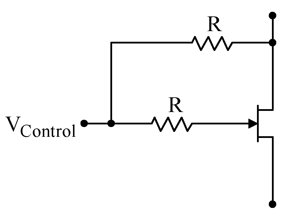
JFET's can be used as variable resistors. IMPORTANT NOTE: The lower resistor R in the diagram at right is in the wrong location; the correct location is shown in Problem 5.8. In this application, the drain source resistance $R_{DS}$ can be controlled by a voltage, $V_\mathrm{Control}$, applied to the gate. With just a JFET, however, this resistance is dependent on the $V_{DS}$, and the "resistor" is nonlinear. It can be shown that the linear-regime resistance $R_{DS}$ between a JFET’s drain and source is given by $\displaystyle \frac{1}{R_{DS}} = 2k{\huge[}(V_{GS}-V_P)-V_{DS}/2\huge]$, where $k$ is a parameter that depends on the individual JFET, $V_P$ is the voltage where the JFET first conducts (the pinch-off, cutoff, or threshold voltage), and $V_{DS}$ is the voltage between the drain and the source. The linearity between $V_{DS}$ and $I_D$ can be restored by adding a signal equal to $V_{DS}/2$ to the gate. This can be done by adding two resistors to the gate circuit as shown to the right. This circuit functions as an excellent variable resistor. Note that this is an application of a JFET being used in the somewhat unusual linear regime as opposed to the more common saturated regime. |
 |
Parasitic Oscillations
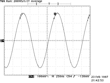
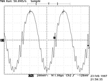
| Parasitic oscillations are unwanted, high frequency oscillations usually caused by unintended positive-feedback loops. The loops are closed by unintended capacitative coupling between two neighboring wires. Because the oscillations normally occur at very high frequencies (1 to 100 MHz), capacitances of only a few picofarads are sufficient to cause oscillations. Parasitic oscillations often first appear as “hair” on an otherwise undistorted signal. For example, in the scope trace on the right, the small oscillations at the top of the original sine wave are due to parasitic oscillations. |
Minor Parasitic Oscillations |
|
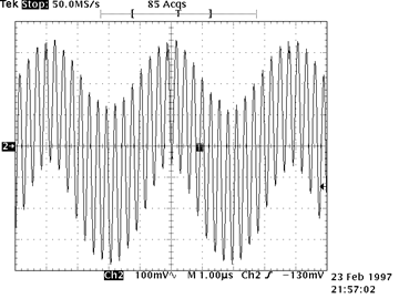
Larger parasitic oscillations may cover a substantial fraction of the signal, as shown to the right, or they may completely dominate the signal, as shown at the extreme right. Touching the circuit, or even waving your hand near the circuit, can either accentuate or suppress the oscillations. Parasitic oscillations generally, but not always, require circuits with gain. The followers that we built in last week’s lab were relatively immune from oscillating, but the amplifiers that you are building this week will likely exhibit paras |
Significant Parasitic Oscillations |
Disasterous Parasitic Oscillations |
There are no hard and fast rules for eliminating parasitic oscillations, but clean circuit layout goes a long way. Keep your leads short and un-jumbled. Lay your signals out from left to right, and keep large output signals away from small input signals. Believe it or not, beautifully wired circuits work better!
Unfortunately not even clean circuit layouts will always suppress the oscillations. At very high frequencies, the internal capacitances inside components, aided by the inductances formed by the component leads, can cause oscillations. An additional feedback route is through the power supplies themselves. Frequently parasitic oscillations can be tamed by liberally adding “decoupling” capacitors across the power supply. The decoupling capacitors function by providing a low impedance path to ground at high frequency, thereby shorting out the high frequency oscillations. To be effective, decoupling capacitors should placed close to the circuit components. Try placing 0.1$\mu F$ capacitors between +12V and ground, –12V and ground, and between +12V and –12V. Vary the locations of the capacitors, and use more than one, until the oscillations go away. Don’t be greedy; a 1 or 10$\mu F$ capacitor will not work better than a 0.1$\mu F$ capacitor. In fact, the larger internal inductances of large capacitors may well make them work worse than smaller capacitors. This is particularly true of electrolytic capacitors.
When power supply decoupling capacitors are insufficient, placing a small capacitor across the input of a circuit will sometimes work.
Packaging and Leads
|
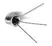
Transistors are manufactured in many different packages and sizes. Our 2N4392 JFETs come in a metal can. (Devices starting with 1N are always diodes; devices starting with 2N are always transistors.) As with many devices, the lead diagram depends on the view. A bottom view (immediate right) looks at the device from the lead side. A top view (center right) looks at the device from the non-leaded side. The 2N4392 leads are arranged in a triangle; the gate lead is the first lead clockwise from the tab when looked at in a top view. When inserting the JFET into the breadboard, there is no need to squash the leads out horizontally. In fact, doing so will risks accidentally shorting the JFET leads to the metal case. Instead of squashing the leads, just bend them out gently so that they form a triangular pattern, and are in different columns on the breadboard. It may be useful to have one of the leads span the breadboard's narrow socketless row region. |
Bottom View |
Top View |
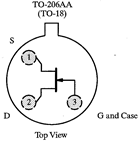 |
 2N4392
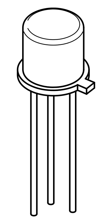
|
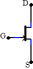
Many JFETs, including the 2N4392, are symmetrically constructed. The source and drain can be exchanged without changing the device behavior. But for simplicity, use should generally use the correct source and drain leads. Asymmetric JFETs, in which the source and drain cannot be exchanged, are normally drawn with an offset gate lead as shown at right. |
 |
In the lab
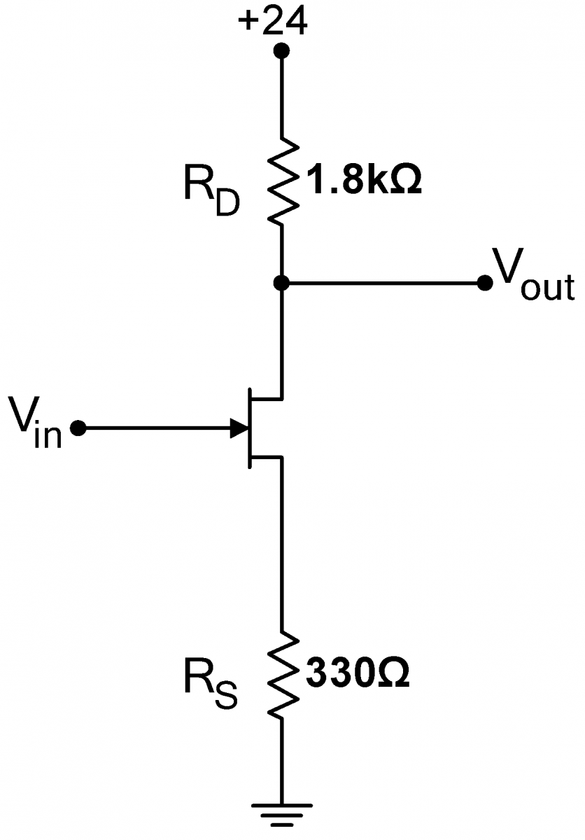
 Problem 5.1 - Common Source JFET Amplifier
|
Construct the amplifier Shown at right. What are the equilibrium voltages and currents in the circuit ($V_{GS}$, $V_{DS}$, $I_{DS}$, $V_{out}$) when $V_\mathrm{in}=0$, i.e. when the input is grounded? Drive the amplifier with a $10\,\mathrm{kHz}$, $0.1\,\mathrm{Vpp}$ sine wave, and look at its output on the scope. What is the amp’s gain? Does it agree with the predicted value? What is the maximum undistorted output amplitude? (Note: Vary the input voltage to search for this quantity.) What limits the amplitude? Cool the JFET with circuit cooler. How much does the gain change? Measure and record the gain for four other JFETs. (Keep all these JFETS for 5.3) |
 |
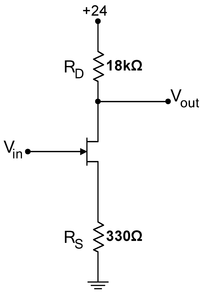
Problem 5.2 - Increased Gain Common Source JFET Amplifier-Large Drain Resistor
|
The gain of the circuit in 5.1 is not high. A naïve application of the gain formula [Eq. (1)] would imply that the gain should increase substantially if the drain resistor is changed to $18\,\mathrm{k}\Omega$, as shown at right. Build this circuit. What actually happens to the gain? Why? (Hint: Remeasure $V_{DS}$). |
 |
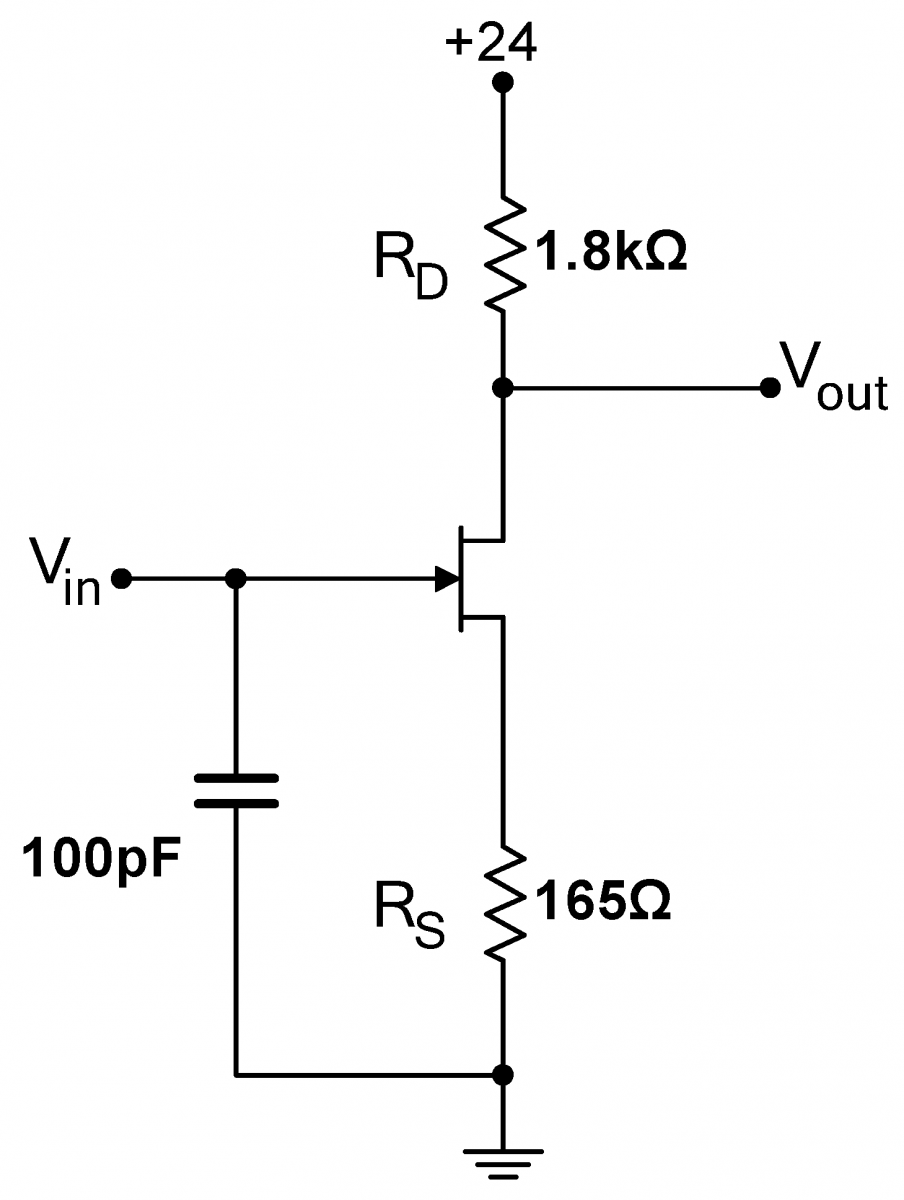
Problem 5.3 - Increased Gain Common Source JFET Amplifier-Small Source Resistor
|
Equation (1) also suggests that decreasing the source resistor will increase the gain. Build the circuit at right. (The $100\,\mathrm{pF}$ capacitor suppresses feedback oscillations, but does not otherwise affect the circuit. Ignore it when calculating the gain.) What is the gain now? Change the input amplitude; what is the maximum undistorted output amplitude? Cool the JFET with circuit cooler. How much does the gain change? Measure and record the gain for the other four JFETs. Why is the fractional variation in the gain larger for this circuit than for the circuit in 5.1? The behavior of a well-designed circuit should not depend on temperature or on the parameters of its particular components. Consequently, the circuit in 5.3 is not very useful. The point of this section is to show you that circuit design is not as simple as plugging in to a formula and getting a useful circuit. |
 |
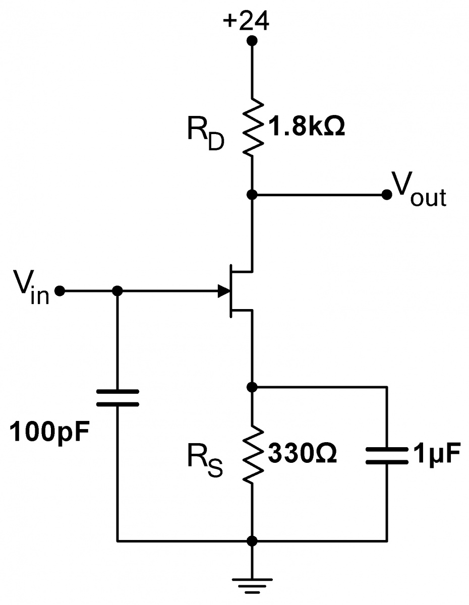
Problem 5.4 - Increased Gain Common Source JFET Amplifier-Source Resistor Bypass
|
Bypassing the source resistor with a capacitor will also increase the gain. Build the circuit at right, which uses a $1\,\mu\mathrm{F}$ bypasss capacitor. Use a regular capacitor, not a polarized electrolytic capacitor. Measure the gain of the circuit. Is the gain frequency dependent? (Particularly explore low frequencies; the high frequency behavior is set by parasitic capacitances which are not interesting in this context.) Why does the capacitor increase the gain? What is the high frequency predicted gain? |
 |
Problem 5.5 - Differential Amplifier
|
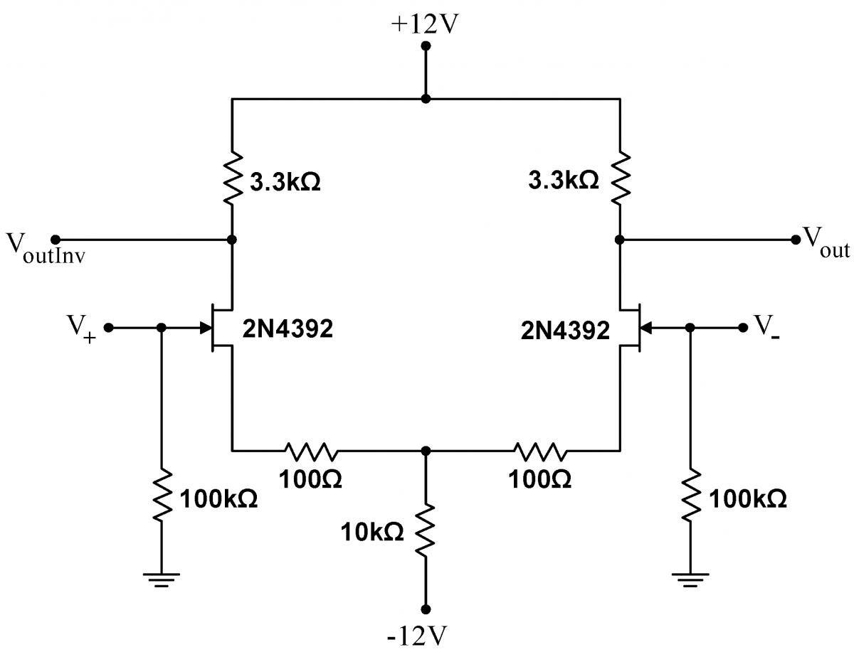
Build the differential amplifier shown at right using your matched pair of JFETs from Lab 4. The $100\,\mathrm{k}\Omega$ resistors establish the inputs near ground, and do not otherwise affect the circuit performance. Note that the power supplies are at positive and negative voltages centered around the ground; this is a very common setup with differential amplifiers. Leaving the $V_-$ input attached only to its $100\,\mathrm{k}\Omega$ resistor, drive the $V_+$ input with a $1\,\mathrm{kHz}$, $0.05\,\mathrm{Vpp}$ sine wave. Measure the amplitude and phase of the output signal $V_{out}$. Also look at $V_{outInv}$; what is the signal there? How do your measurements compare to the values predicted by Eqs (2) and (3)? Reverse the drive setup; drive the $V_-$ input and let $V_+$ be grounded through its $100\,\mathrm{k}\Omega$ resistor. What are the amplitude and phase at $V_{out}$? What about at $V_{outInv}$? Now drive $V_+$ and $V_-$ with identical signals (short them together). What is the common mode gain? If your circuit does not work, particularly if only one branch of the circuit works slightly and the other not at all, it is likely that your JFETs are not sufficiently well matched. Explore this effect by temporarily replacing one of the JFETs with an unmatched JFET. Does the circuit still work? If it doesn’t, why not? Hint‑Measure the voltage drop across both drain resistors. |
 |
Problem 5.6 - Improved Diffential Amplifier
|
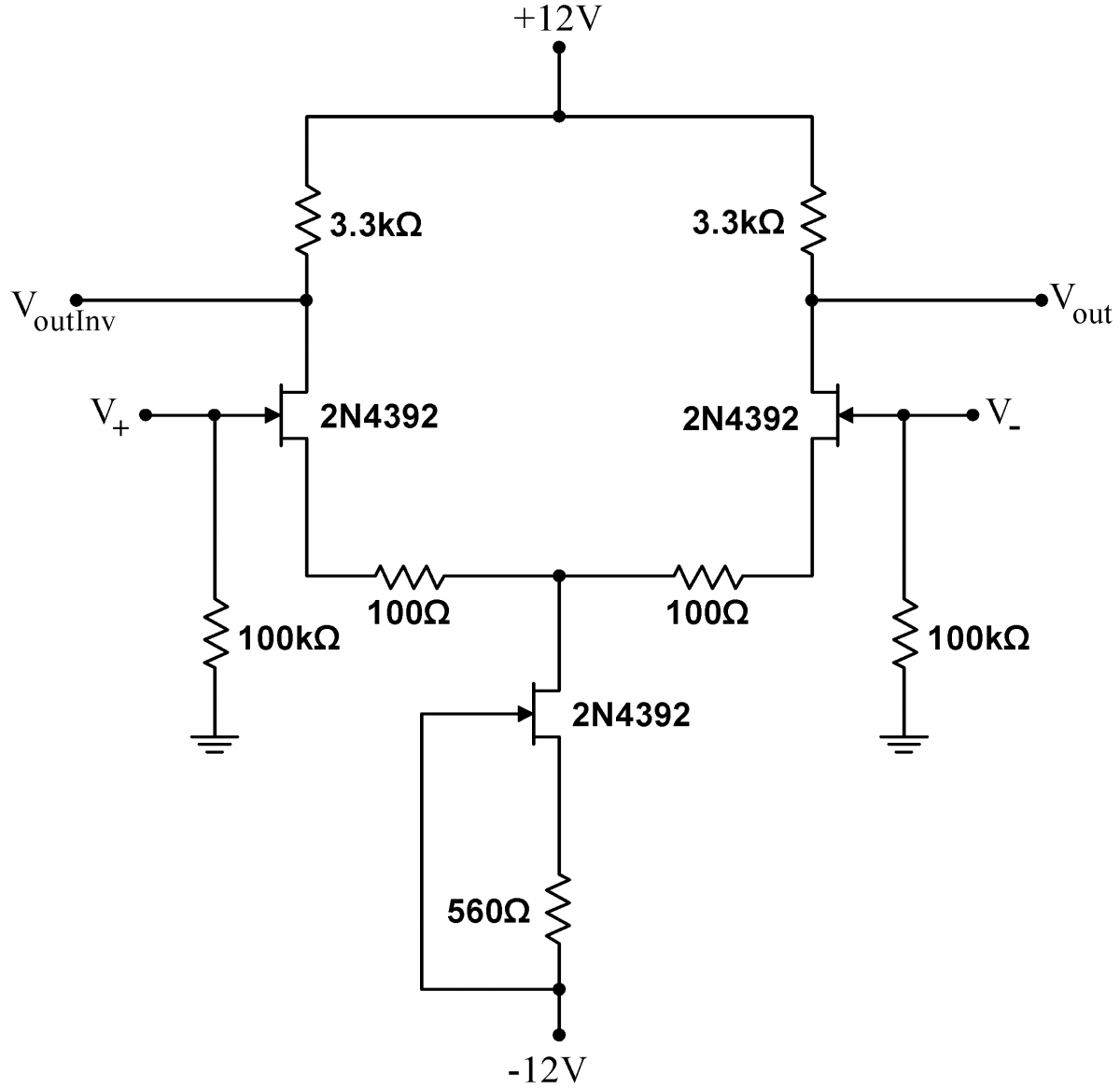
Differential amplifier performance is vastly improved by replacing the common source resistor with a current source. Make all the measurements in 5.5 with the circuit at right. Note that Exercise 5.13 uses the matched JFETs again, so make sure that you keep them. |
 |
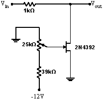
Problem 5.7 - JFET Attenuator
|
Build the JFET attenuator shown at right. This circuit looks like a voltage divider. The "top" resistor in the divider is the $1\,\mathrm{k}\Omega$ resistor between $V_\mathrm{in}$ and $V_\mathrm{out}$, while the base resistor is the JFET. As discussed in the background information, the JFET $R_{DS}$ can be controlled by the voltage on the gate, here adjusted with the potentiometer. Drive $V_\mathrm{in}$ with a $1\,\mathrm{kHz}$, $0.05\,\mathrm{Vpp}$ triangle wave. Show that you can vary the output amplitude $V_\mathrm{out}$with the potentiometer. Is the circuit linear (i.e. is the output still a good triangle wave)? With the potentiometer set to produce an output signal about half as large as the input signal, what is the largest input signal passed relatively undistorted? Hint for 5.7 and 5.8: If you find that your circuit always attenuates, i.e. you cannot make $V_\mathrm{out}\approx V_\mathrm{in}$, try replacing the $39\,\mathrm{k}\Omega$ resistor with a smaller resistor. |
 |
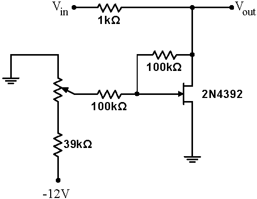
Problem 5.8 Linearized JFET Attenuator
|
You should have found in 5.7 that the attenuator became nonlinear at higher $V_\mathrm{in}$ amplitudes linear. Build the circuit at right, which contains two $100\,\mathrm{k}\Omega$ resistors, and which should linearize the attenuator. With the potentiometer set to produce an output signal about half as large as the input signal, find the largest input signal passed relatively undistorted. Is the amplitude larger than in 5.7? Now set the potentiometer for the greatest attainable attenuation. Measure the resulting attenuation, and from this measurement and the standard voltage divider formula, calculate the JFET drain-source resistance $R_{DS}$. This is the lowest possible $R_{DS}$ for the JFET, a parameter that is often given on the JFET spec sheet. |
 |
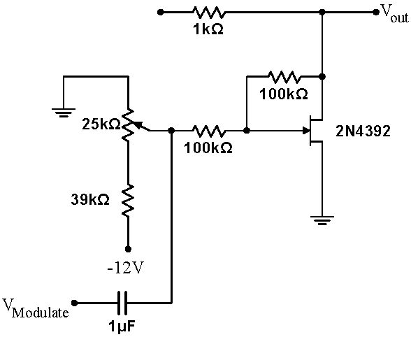
Problem 5.9 - JFET Modulator
|
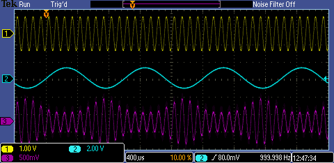
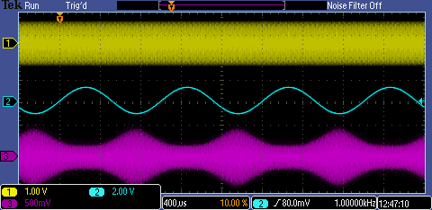
The circuit in 5.8 uses a fixed control voltage on the JFET gate, and, consequently, yields a constant attenuation. However, this not a requirement; if the signal on the JFET gate is driven with a time dependent signal, the attenuation will then be time dependent as well. Build the circuit at right. Drive $V_\mathrm{in}$ with a $1\,\mathrm{MHz}$, $1\,\mathrm{Vpp}$ sine wave from your signal generator. In this setup, this $1\,\mathrm{MHz}$ wave is called the carrier wave. Drive the $V_\mathrm{Modulate}$ input with an audio frequency ($1\,\mathrm{kHz}$), $1\,\mathrm{Vpp}$ sine wave. Since we only have one function generator per station, the distribution boxes with BNC outputs labeled "T1" and "T2" have been set up to provide you with the extra signal. Specifically, T1 should be a 1 kHz sine wave, and T2 should be an audio signal. If they are not outputting any signal, a GSI may need to set up the amplifier that distributes them to the room. Setup the scope with the $V_{in}$ signal on channel 1, the modulation signal $V_\mathrm{Modulate}$ on channel 2, and the output signal $V_\mathrm{out}$ on channel 3. Trigger the scope on $V_\mathrm{Modulate}$. Adjust the potentiometer until you see a modulated carrier wave on $V_\mathrm{out}$ : the envelope (local amplitude) of the high frequency carrier wave should be related to the instantaneous amplitude of the audio signal. The output $V_\mathrm{out}$ of the circuit should then be proportional to $\displaystyle \big( 1+\epsilon\sin\omega_1t\big) \sin\omega_0 t$, where $\omega_0$ is the radial frequency of the $1\,\mathrm{MHz}$ carrier wave, $\omega_1$ is the radial frequency of the $1\,\mathrm{kHz}$ audio wave, and $0<\epsilon<1$ is called the amplitude of the oscillation. The signals should look like the lower right scope traces. When you attain a properly modulated signal, record the scope traces.. This type of circuit is called a modulator, and has many uses.
|
 |
|
Modulated $10\,\mathrm{kHz}$ Carrier
|
 Problem 5.10 - JFET AM Transmitter
|
Attach a 2-meter long wire to the output of the modulator you built in 5.9. Obtain an AM radio, place the antenna very near the radio, and tune it to a quiet frequency in the AM band. Adjust the high frequency carrier signal until you can hear the 1kHz tone coming from the radio. Then replace the sine modulating signal from T1 with the audio signal from T2. Listen to the radio. You have built a low power AM transmitter! Note that you can extend the range of your transmitter by turning up the amplitude of your $1\,\mathrm{MHz}$ carrier wave. |
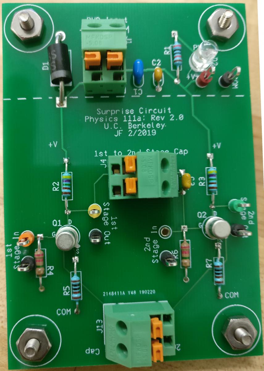
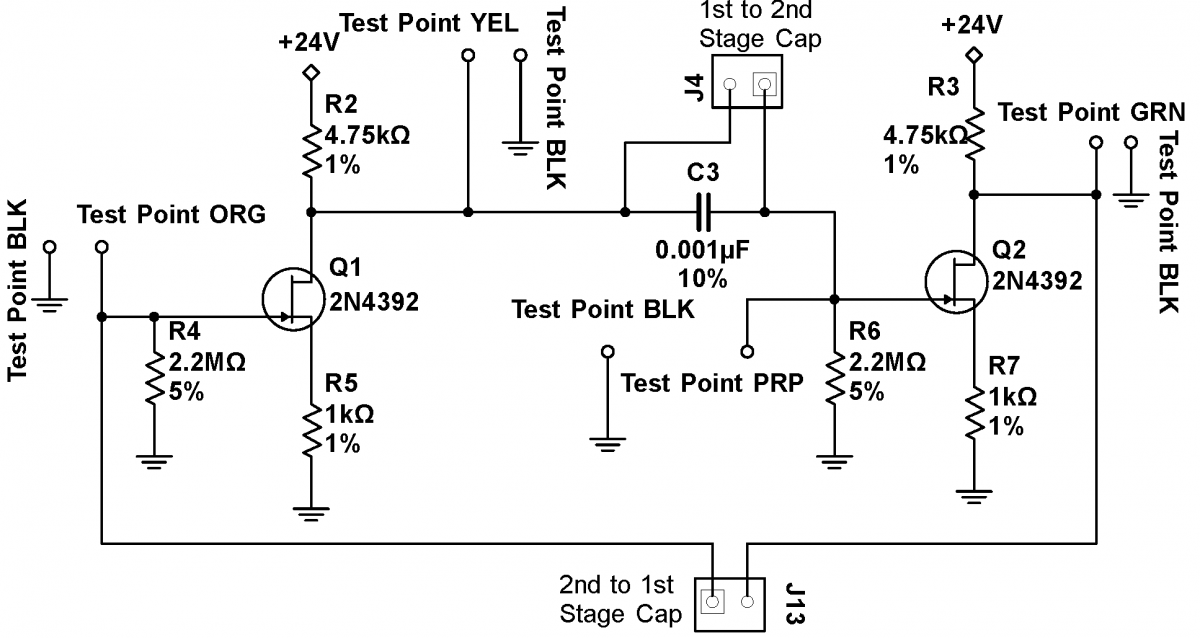
Problem 5.11 - Surprise Circuit
|
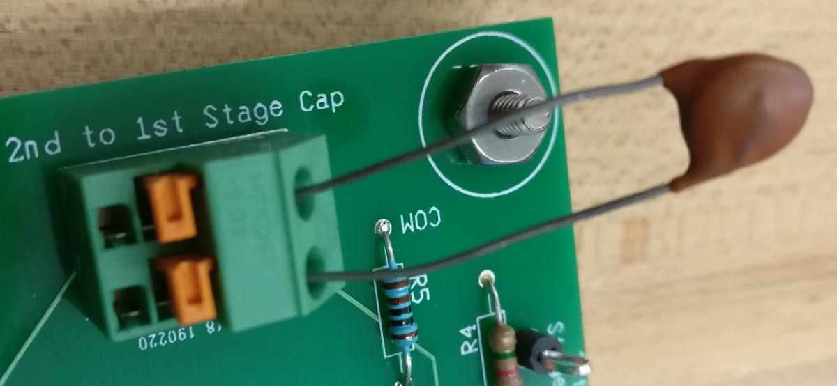
Obtain a printed circuit board (PCB) marked "Surprise Circuit Physics 111a: Rev 2.0, as pictured at right. The schematic for the circuit below the dashed line is also shown at right. (The circuitry above the dashed line on the PCB cleans and decouples the power and need not concern you except while confirming the power. Use the breadboard box power supplies to generate approximately 24-27V, and use a set of leads (preferably twisted) to connect this power to "PWR Input Block". Wires can be inserted into this Block in a manner similar to the way you inserted wires to the block on the Thevenin circuit. Insert stripped wires into the round holes while simultaneously depressing the orange tabs. It takes some force to depress these tabs, but treat them gently nonetheless. Make sure that you use the proper polarity. Remove any components that might be inserted into the "...Cap" connector blocks. Power the circuit to confirm the red power LED lights. Further confirm, by measuring the voltage across the red and black test points at the top, that the power you are applying to the circuit is what you would expect. Note that black test points are always grounded. In all cases making measurements with the scope, connect the scope ground to one of the black testpoints. Inject a 100mV, 3kHz sine wave into the "1st State In" orange test point. Attach a scope (on AC) to the "1st Stage Out" yellow testpoint. Measure the approximate gain. Is the output signal inverted or non-inverted? Now move the injected sine wave to the "2nd Stage In" purple test point (the purple and black test points are difficult to distinguish) and the scope to the "2nd Stage Out" green test point. Measure the approximate gain. Is the signal inverted or non-inverted? Finally, move the injected sine wave back to the "1st State In" orange test point while leaving the scope on the green test point. Is the gain what you would expect given that the two stages are coupled through the 0.001 capacitor? (The value of the capacitor does not significantly affect the gain at 3kHz.) More importantly, is the signal inverted or non-inverted? Now remove the injected sine wave while keeping the scope on the "2nd Stage Out" green testpoint. Insert a 100pF capacitor across the "2nd to 1st Stage Cap" terminal block (see bottom at right). What do you observe on the scope? Concentrate on the frequency and shape of the waveform, not its amplitude. Play with different values of the "2nd to 1st Stage Cap" capacitor, going down to 10pF, and up to 10nf. Try inserting a capacitor across the "1st to 2nd Stage Cap" (this inserted capacitor will be in parallel to the 0.001uF capacitor C3). Can you make qualitative sense of the changes to the output that you observe?
|
|
Problem 5.12 - Phase Splitter
Design and build a unity gain phase splitter: a circuit that splits an input signal into two signals of equal magnitude and opposite phase. Maximize the undistorted output amplitude of your circuit. Hint: Your circuit should be fairly simple; you do not need a differential amplifier. A modified source follower will work.
Problem 5.13 - High Gain Amplifier
|
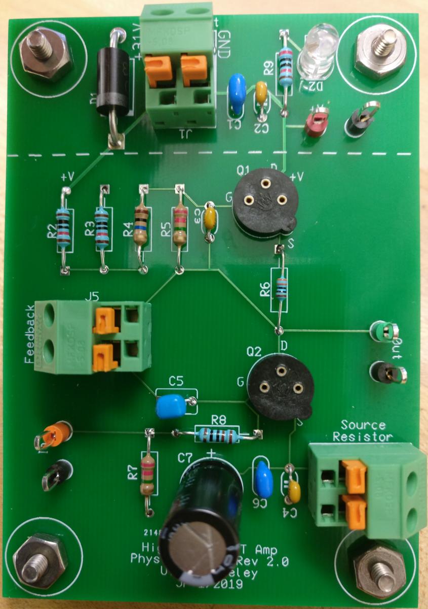
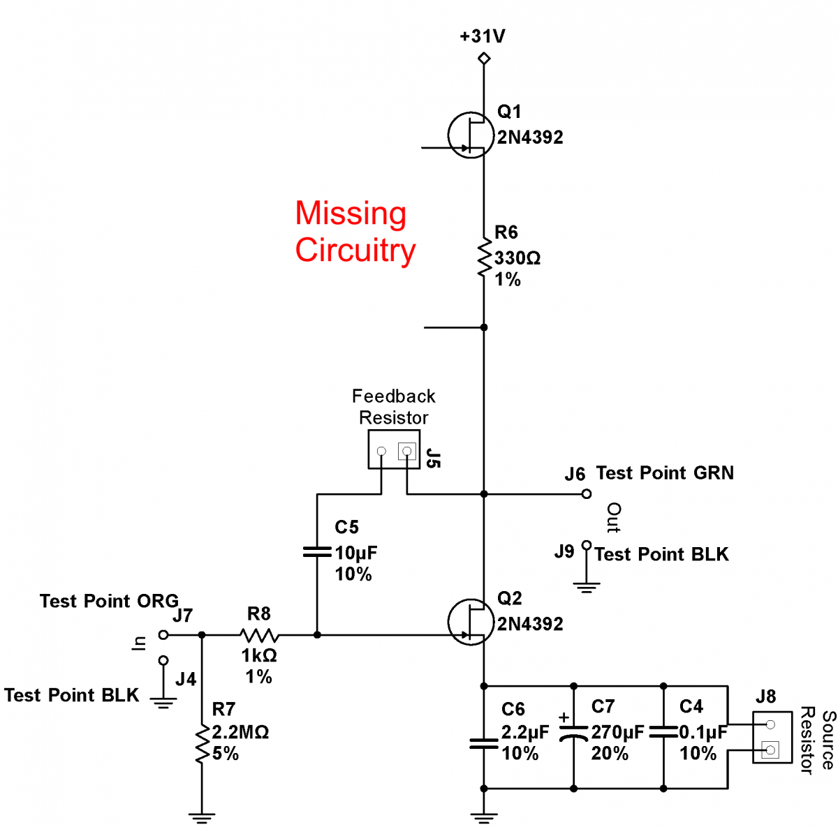
With a careful design employing feedback, it is possible to make a high gain amplifier with constant gain across a wide frequency span and with a gain that is component independent. During this exercise, work the 5.14 questions in tandem. Obtain a printed circuit board (PCB) marked "High Gain JFET Amp Physics 111a: Rev 2.0 as shown at right A partial schematic for the circuit is also shown at right (note that this circuit is not entirely identical to the circuit in the "old" version.) A useful skill is the ability to reconstruct a circuit on a board by tracing the "wires". ( Wires are called traces on a PCB.). The two-layer board used in this exercise is particularly simple. All the traces except the ground connections are on the top surface. The trace are easily visible, though, except where the components are soldered, the traces are covered with a green, transparent insulator. The entire bottom surface of the PCB is a sheet of copper called a ground plane, and components that need to be grounded are soldered directly to this ground plane. You can almost always reconstruct the circuit for a two-layer board like this; it becomes much harder, often impossible, for a board that has traces sandwiched into the middle of the board; such a board is called a multilayer board. Visually, perhaps with the assistance of the multimeter, reconstruct the missing pieces of the circuit diagram. Ignore all the power supply components above the dashed line. Connect power to the "PWR Input" Block, much as you did in exercise 5.11, but use approximately 31V, not 26V. Confirm that the power is properly attached as in exercise 5.11. Note that black test points are always grounded. In all cases making measurements with the scope, connect the scope ground to one of the black testpoints. Insert your matched JFETs into the two black sockets Q1 and Q2. Make sure that you get the orientation correct. The tab on the socket must match the metal tab on the JFET. Calculate the value of the resistor that you need to attach to the "Source Resistor" Input Block to make the voltage midway in the circuit, at Test Point GRN, approximately half the total voltage, i.e. about 15.5V. Obtain and insert this resistor. (When looking for the proper resistor, don't forget the precision (1%) resistor stash by the lab entrance door.) Leave the "Feedback Resistor" Input Block open. Turn the power on. Check to make sure that the DC voltage at the green testpoint marked Out is near 15.5V. Inject a 10mV, 3kHz sine signal into the circuit at the orange test point marked In. Connect the green Out testpoint to a scope. The output signal will be centered around 15.5V, so use AC coupling on the output scope channel. Measure and record the gain at 3kHz. Then measure and record the gain from 3kHz down to 1Hz and then from 3kHz up to 1MHz. (You will find it easier to scan up and down from 3kHz, where the signal is initially large, than from 1Hz to 1MHz in one pass.) You need take only approximately two points every decade, though consider taking slightly more dense points when the gain is changing quickly. Use averaging when neccessary, and aux triggering on Normal, not Auto. (Note that at low frequencies, the AC coupling will affect the signal magnitude. Compensate for this by measuring the size of the input signal as well as the output signal on AC coupling. Since the frequency response of both scope channels will be the same, this response will cancel out of the gain calculation.) The gain should be quite high (over 100) in the neighborhood of $10\,\mathrm{kHz}$ 3kHz. Find the approximate maximum gain frequency, as well as the span around this frequency for which the gain is 80% or more and 50% or more of the max gain. Now set the frequency to 3kHz, and calculate an appropriate feedback resistor value to make the total gain about 15. Insert this resistor into the "Feedback Resistor" Block. If the value is off, adjust the resistor value to be close to 15; aim to be somewhere between 13 and 17. Now redo the frequency scan between 1Hz and 1MHz. Find the approximate maximum gain frequency, as well as the span around this frequency for which the gain is 80% or more and 50% or more of the max gain. Plot the gain with and without feedback. Though the gain is much lower with feedback, you should find that it varies much less over the frequency range than the gain without feedback. Set the frequency back to 3kHz. Insert and measure the gain for several different JFETs swapped in for the lower JFET (Q2) with the feedback resistor removed. Calculate the average gain, and the proportional standard deviation (the standard deviation divided by the average). Put back the feedback resistor. and try the same sample of different JFETs. Calculate the average gain and the proportional standard deviation again. Is the proportional standard deviation much lower with feedback? Finally, change the input to a 1kHz square wave. With your matched JFET, compare the output waveforms with and without feedback. Is the waveform cleaner, with sharper rises and falls (i.e. closer to an ideal square wave) with feedback? Take scope images with both conditions. |
|
Problem 5.14 - High Gain Amplifier Explanation
In the circuit of 5.14, identify the components that perform the following functions, and explain how each function is accomplished:
1. Sets the gain through feedback.
2. Acts as a current source to increase the gain.
3. Increases the open-loop gain by bypassing the source resistor.
4. Sets the current through the JFETs.
5. Assures that the drain source voltage across both JFETs is approximately 12V, independent of the particular parameters of each JFET.
6. Increases the stiffness of the current source by providing a bypass for AC signals.
Problem 5.15 - Improved Differential Amplifier Gain
What are the expected common mode and differential gains for a differential amplifier built with a current source? How do these expected gains compare to the gains you measured in 5.6? Hint‑You will have to assume a stiffness (or Zout) for the source.
Please fill out the