Lab 3 - Diodes
University of California at Berkeley
Donald A. Glaser Physics 111A
Instrumentation Laboratory
Lab 3
Semiconductor Diodes
© 2015 by the Regents of the University of California. All rights reserved.
|
Art of Electronics Student Manual, Hayes & Horowitz |
Pages 65–69, 71–74, 76–78 | |
| The Art of Electronics, Horowitz & Hill | Chapter 1.6, Appendix F | |
| Lab notes | Sections on Small Signal Input and Output Impedance in the Linear Circuit I lab | |
| Various other books | Readings |
Physics 111-Lab Library Reference Site
Reprints and other information can be found on the Physics 111 Library Site.
Lab 3 Appendices: Data sheets and Curve Tracer operation.
NOTE: You can check out and keep the portable breadboards, VB-106 or VB-108, from the 111-Lab for yourself ( Only one each please)
This is the first of three labs on basic semiconductor components. You will study semiconductor characteristics and some of their applications, leading up to the design and construction of a differential amplifier. Note: Keep all your parts with you, as they are for you permanently.
DO NOT RETURN THEM TO THE CABINETS.
This lab studies diodes. You will find the relationship between the voltage and current in a diode, and study temperature effects, rectification, nonlinear phenomena, and frequency doubling.
This lab uses liquid nitrogen (LN$_\mathrm{2}$), which is very cold: approximately $77\,\mathrm{K}$. LN$_\mathrm{2}$ can cause severe skin and eye "burns". Use Safety Goggles while working with LN$_\mathrm{2}$; goggles are provided free in the 111-Lab and are yours to keep. Open-toe shoes are not permitted in the lab while LN$_\mathrm{2}$ is in use.
Read the Cryogenic safety materials from EH&S. Take the cryogenic training: Go to https://uc.sumtotal.host/Core/search and enter 109 in the search window. You may need to select UCB and then login. ~~~ (Alternatively, you may be able to get into the training via http://blu.berkeley.edu , Login, then click UC Learning Center in the left hand column, and then when the UC Learning Center opens click Find A Course, enter 109 in the search window that opens up and click Search. You should now see EHS 109 Cryogens Safety which you can click to enter the training.) ( Yet another way in is https://jwas.ehs.berkeley.edu/lmsi which links from https://ehs.berkeley.edu/training/uc-learning-center-access and then click Find A Course and then search 109 )
If you cannot log into blu nor sumtotal, please show your issue to your instructor or GSI. If they see no obvoius fix please capture a screenshot or snip of the issue and upload this along with your name and email via the form:
https://app.smartsheet.com/b/form/ecc351889e484beb99f77dc0dc0d5d59 (Please check the box that says "Send me a copy of my responses" and then forward the email your receive to winthrop@berkeley.edu)
Obtain the LH$_\mathrm{2}$ from a GSI, who will provide it for you in a styrofoam cup. Be careful not to spill the cup. You are not allowed to obtain the LN$_\mathrm{2}$ form the storage dewar yourself.
The semiconductor components used henceforth in this course can get quite hot...especially if they are hooked up incorrectly. They can easily burn you. If you must touch components while the power is on, touch them gingerly first to asses their temperature before grasping them with force. Better yet, turn the power off, and wait a few moments for the components to cool down.
Before coming to class complete this list of tasks:
· Completely read the Lab Write-up
· Answer the pre-lab questions utilizing the references and the write-up
· Perform any circuit calculations use Matlab or anything that can be done outside of lab use RStudio (freeware). [NOTE added: R is now a dead language. Learn Python instead.]
· Plan out how to perform Lab tasks.
All part spec sheets are located here the Physics111 Library site
Pre-lab
1. In a few sentences, explain what diodes are and how they are useful.
2. Show that the second term in Eq. (1) (the $-1$ in the brackets) may be neglected for typical operating parameters:
$V>0.1\;V,\;kT\approx\frac{1}{40}eV,\;n\approx 2$.
3. Why is there a ripple on top of the DC voltage output by the circuit in 3.11?
4. What is a load line used for? What are the relative advantages of graphical and iterative analysis?
This lab is one of the most analysis and plotting intensive labs done this semester. Do not leave your analysis section to the last minute. Using a computer to do the analysis is much easier & quicker than doing it by hand. Bring a thumb drive to class or alternatively e-mail yourself the data files from the diode characteristic traces found by the Curve Tracer so you will have access to data both at your lab station and home. Excel is a powerful timesaver when graphing similar data sets multiple times.
Light Emitting Diodes (LEDs) will burn out if you hook them directly to the 5V power supply without a current limiting resistor.
Background
Diodes and pn Junctions
Diodes and transistors are made from semiconducting materials: typically crystalline silicon. Pure silicon has few free electrons and is quite resistive. To increase its conductivity, the silicon is normally "doped", i.e. deliberately contaminated, with other elements. Some dopants, like phosphor, arsenic and antimony, easily give up one of their electrons to the now impure silicon crystal. These donated electrons are free to move about the crystal, and its conductivity increases dramatically. Only a few dopant atoms will significantly increase the crystal's conductivity. For example, one dopant atom per 100 million silicon atoms will increase pure silicon’s conductivity by approximately 105. Of course, dopants atoms that give up an electron become positively charged. The net charge remains zero.
Other dopants, like boron, indium and aluminum, grab electrons from the surrounding silicon atoms, leaving positively charged silicon ions behind. In turn, these now positive silicon ions try to regain their neutrality by grabbing electrons from their neighbors…the net result is that there are regions of “positiveness” floating around the crystal lattice. Such “absences of electrons” are called holes. Amazingly, holes behave almost exactly like positively charged electrons; they move, respond to electric fields, and appear to have a mass close to the electron mass.
A doped semiconductor with more mobile electrons than holes is called an “n‑type” semiconductor; conversely, a doped semiconductor with more holes than mobile electrons is called a “p‑type” semiconductor.
If doping’s only effect was to increase semiconductor conductivity, semiconductors would be obscure, little-used materials. The utility of semiconductors comes from the remarkable effects of placing p and n‑type materials next to each other. Such juxtapositions are called “pn” junctions. An isolated pn junction makes a semiconductor diode. Other semiconductor components are made from more complicated arrangements; bipolar npn transistors, for example, are made by sandwiching a p layer in between two n layers, hence the name npn.
The current through an ideal pn junction is given by the diode equation.
$\displaystyle I(V)=I_\mathrm{sat}\bigg[\exp\bigg({\frac{eV}{nkT}\bigg)}-1\bigg],$ (1)
where $V$ is the voltage drop across the junction, $I_\mathrm{sat}$ is a constant called the saturation current and depends on the temperature, on the particular geometry of the junction, and on the material of the junction, $e = 1.6\times10^{-19}\,\mathrm{C}$ is the charge of an electron, $k = 1.38\times10^{-23}\,\mathrm{J/K}$ is Boltzmann’s constant, and $T$ is the temperature in Kelvin. (A good approximation to memorize is that at room temperature, $kT\approx 1/40\,\mathrm{eV}$.) The constant $n$ varies between 1 and 2 depending on the particular diode, but is typically equal to 2 for discrete diodes.
Notice from Eq. (1) that the diode’s response is directional and highly nonlinear. When forward biased, ($V$ positive) enormous currents can flow through the diode because of the exponential dependence of $I$ on $V$. When the diode is reverse biased, ($V$ negative), the current then approaches $-I_\mathrm{sat}$. Since $I_\mathrm{sat}$ is typically very small (picoamps are not uncommon), very little current flows. Thus the diode acts like a one-way valve; current can only flow in one direction.
Be aware that while Eq. (1) properly describes the diode voltage dependence, the implicit temperature dependences in $I_\mathrm{sat}$ dominate over the explicit dependence in Eq. (1). For example, the current typically goes down, not up, as the temperature decreases.
|
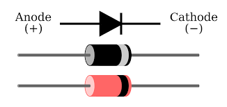
When forward biased, the positive end of the diode is called the anode, and the negative end is called the cathode. The terms anode and cathode date from the days of vacuum tube diodes. The symbol for a diode is shown at right. The direction of the "arrow" indicates the direction of current flow. On an actual diode, the cathode is normally marked with a painted band as also shown at right. This band can be hard to see on some of our diodes. Light emitting diodes (LEDs) are marked differently; the cathode is the shorter lead (but make sure that the leads have not been trimmed), or, on some LEDs, the lead adjacent to the flat on the plastic housing. |
after commons.wikimedia.org |
Nonlinear Circuit Equilibrium
Unlike purely linear circuits, circuits containing nonlinear elements like diodes cannot be reduced to systems of linear equations. Consequently, the equilibrium voltages and currents in nonlinear circuits are much more difficult to determine. Although these equilibrium quantities can be found using complicated computer programs like MultiSim, quick, approximate analysis methods are often useful, particularly for simple circuits. Two quick methods will be used in this course: (I) Graphical Analysis and (II) Iterative Analysis
(I) Graphical Analysis – Load Lines
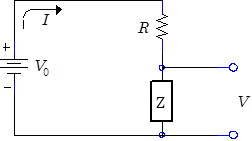 Consider the simple circuit at right which contains a voltage source $V_0$, a resistor $R$ and a generic nonlinear component with impedance $Z(V)$, where $V$ is the voltage across the component. Regardless of behavior of the nonlinear component, the voltage source and resistor set certain constraints on the possible equilibrium voltages and currents. For instance, the current $I$ cannot exceed $V_0/R$, the current that flows when the impedance of the nonlinear component $Z$ is zero. Under these conditions, the voltage $V$ across the nonlinear component is zero. Alternately, $V$ cannot exceed the voltage of the source $V_0$ , and this maximum voltage is only obtained when the impedance $Z$ is infinite and $I=0$. Impedances between zero and infinity produce intermediate values of the current and voltage. (We have assumed here that the nonlinear device does not contain any internal power source, hence $\mathrm{Re}(Z)\geq0$.)
The possible values fall on a curve given by the parametric equations $I=V_0/(R+Z)$ and $V=ZV_0/(R+Z)$, where $Z$ varies between zero and infinity. Eliminating $Z$ demonstrates that the curve is actually a straight line given by the equation
$\displaystyle I(V)=(V_0-V)/R$. (2)
This equation could have been derived directly from its end points, $I=V_0/R$ at $V=0$ and $I=0$ at $V=V_0$. The line determined by Eq. (2) is called the load line because it is determined solely by the load (and the power source), not by the nonlinear component.
The nonlinear component obeys its own equation, or “characteristic” curve $I_Z(V)$. In equilibrium, both the load line and the characteristic curve must be satisfied simultaneously. Consequently the equilibrium current and voltage for the circuit are given by the intersection of the load line (Eq. (2)) and the characteristic equation $I_Z(V)$.
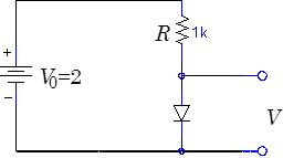
For example, assume that the nonlinear component is a diode ($I_\mathrm{sat}=4\times10^{-10}\,\mathrm{A}$) driven by a $1\,\mathrm{k}\Omega$ 1k resistor from a $2\,\mathrm{V}$ battery, as shown below left. The load line and diode characteristic (Eq. 1) for this circuit intersect, as shown below right, at equilibrium voltage $V=0.75\,\mathrm{V}$ and current $I= 1.25\,\mathrm{mA}$.
|
Fig. 1: Resistor Diode Equilibrium |
Fig. 2: Load Line Analysis |
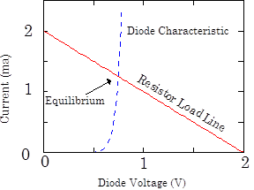
The equilibrium voltage and current across the diode is sometimes called the operating point of the circuit.
(II) Iterative Analysis
|
Nonlinear equilibria can also be found iteratively: by guessing an initial solution, determining the consequences of the guess, and then iteratively refining the guess. This method is best explained with an example: Using the diode circuit in Fig. 1, guess a current (say $I=5\,\mathrm{mA}$), and then invert the diode characteristic $\displaystyle V(I)=(nkT/e)\ln{(1+I/I_\mathrm{sat}})$ to find the voltage across the diode that would have produced this current,$V=0.81706\,\mathrm{V}$. Next subtract this voltage from the battery voltage to determine the voltage across the resistor $V_0-V=1.18294\,\mathrm{V}$, and divide by the resistance $R$ to refine the current guess to $1.18294\,\mathrm{mA}$. Repeat and continue iterating until the numbers converge. The first five iterations are given in the table at right. The results have converged to six decimal places. |
|
The apparent precision of the iterative method is deceptive as it relies on precise knowledge of $I_\mathrm{sat}$ and $n$. Don’t worry; answers with accuracy's better than 10% are rarely required in electronics.
[Be careful: iterative methods do not always converge. In fact, running the described sequence backwards (guess the diode voltage, calculate the current, find the resistor voltage drop, and subtract from the battery voltage to refine the diode voltage guess) does not converge. Try it yourself! The study of the convergence of these methods is called Iterated Map Theory, and, surprisingly, is the basis for Chaos Theory.]
Both the load line analysis and the iterative analysis yield the same values for the equilibrium voltage and current. Note that the diode equation [Eq. (1)] was used in both methods. With some loss in precision, experimental data taken from an actual diode can be used instead.
Perturbation Analysis
Determining a circuit’s response to small changes in its parameters is as important as determining its initial equilibrium. The general subject of the response of a system to small parameter changes (perturbations) is called perturbation analysis. In the circuit of Fig. 1, for example, perturbation analysis can be used to determine the change in the diode voltage when small changes are made to the source voltage.
(I) Graphical Perturbation Analysis
|
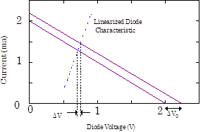
By definition perturbation analysis considers only small changes to the system parameters. Consequently it is both convenient and permissible to linearize around the equilibrium conditions. Thus, a curved characteristic curve becomes a straight line. Using the circuit in Fig. 1 as an example, consider a small change in the battery voltage of $\Delta V_0=+0.25\,\mathrm{V}$. This perturbation will shift the load line upwards as shown at right, and the intersection will shift concomitantly. The change in the diode voltage $\Delta V=0.0088\,\mathrm{V}$ can then be read off the graph from the new intersection point. In this case, $\Delta V$ is much smaller than the change in the battery voltage $\Delta V_0$. (For graphical clarity, the slope of the linearized diode characteristic has been decreased; otherwise $\Delta V$ would have been so small as to be unreadable.) |
Fig. 3: Perturbation Analysis |
(II) Small Signal Impedance Perturbation Analysis
The above graphical procedure is completely equivalent to the following method: First calculate the small signal impedance $z$ of the nonlinear diode at its operating point. The small signal impedance is the reciprocal of the slope of the diode characteristic curve at the operating point.
$z=\dfrac{\partial V}{\partial I}\bigg|_{operating\;point}$.
Then use $z$ in a “linear” circuit analysis. Because the characteristic curve is not linear, $z$ must be recalculated if the voltage across the diode changes (i.e. if the operating point changes).
For more information, see http://en.wikipedia.org/wiki/Small_signal_model
In the lab
Problem 3.1 - Forward and Reverse Diode Behavior
|
Obtain a 1N4448 diode. The label 1N4448 designates the type of diode. Tens of thousands of different types of diodes are available. Many types are made by several different manufacturers; each manufacturer certifies that their diode meets the industry-wide specifications. Parts with labels that begin with 1N are always diodes, while parts that begin with 2N are transistors, but not all diodes and transistors follow this naming convention. Specifications for the 1N4448 diode are on the Physics Library site. This lab also uses another type of diode, the 1N5234B which is very difficult to differentiate from the 1N4448 visually. Make sure that you do not mix up the two types, and make sure that you return your diode to the proper drawer. |
 |
Use a Double Banana plug, a BNC cable and minigrabbers to connect the DMM to the diode. Set the DMM to the diode scale. (On the handheld Fluke DMM, this is the scale indicated by the yellow diode symbol 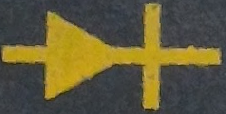 ; make sure that you press the yellow "shift" button to toggle between this scale and the continuity scale. On the benchtop Kiethley DMM, this is the scale indicated by the blue diode symbol
  ; make sure that you use press the blue "shift" button before you go to this scale.)
With the Double Banana plug ground hooked up to the COM (Fluke) or LO (Keithley) Banana input plug, the red minigrabber lead will be positively biased referenced to the black lead; thus, for diode conduction, the red lead should be attached to the diode anode, and the black lead should be attached to the cathode. On the diode itself, the cathode is marked by a black band; in the 1N4448 image above, the band is at the bottom.
The DMM diode settings attempt to impress $1\,\mathrm{mA}$ through the diode, while simultaneously measuring the voltage across the diode. If the diode is forward biased, the voltage measurement will be the "forward voltage drop" of the diode at $1\,\mathrm{mA}$. If it is reversed biased, the maximum output voltage of the DMM (about $7\,\mathrm{V}$ for the Fluke, and $2.5\,\mathrm{V}$ for the Keithley) will be insufficient to drive $1\,\mathrm{mA}$, and the meter will read an error code (OL for the Fluke, and Open for the Keithley).
Confirm that the diode conducts unidirectionally by measuring the forward voltage drop when the diode is forward biased, and an error code when the diode is reversed biased. You should get a forward voltage drop on the order of $0.6\,\mathrm{V}$.
 Problem 3.2 - Forward Voltage Drop Temperature Dependence
Obtain a plastic-stick-mounted 1N4448 diode from the laboratory staff. Repeat your measurement of the forward voltage drop using the DMM. Does this diode have exactly the same forward voltage drop as the diode you used in part 3.1? Forward voltage drops vary between types of diodes and even between diodes of the same type.
Squeeze the diode between you fingers. The forward voltage drop should change as the diode heats up to your finger temperature. What is the new value? For more dramatic results, dip the diode into liquid nitrogen, which you can obtain from the laboratory staff. What is the forward voltage drop now? Diodes are frequently used as temperature sensors by measuring this forward voltage drop.
Warning: Because diodes of the same type can have significantly different characteristics, use the same diode for all experiments in this lab. If you need to use your diode on another day, mark it with a piece of tape with your name and leave it in the storage cubbies in the back of the lab.
Problem 3.3 - Offset Adder Functionality I
Now examine the behavior of the Offset Adder circuit included on the breadboard box at your lab station. A picture of the offset adder, and a brief description of its functionality, cae be found in the Lab 1 manual immediately after Problem 1.1.3.
Temporarily ignore the input BNC jack. Measure the output voltage (from the BNC output jack) while turning the Offset Adjust knob. See how the voltage can be varied from approximately $-9$ to $+9\,\mathrm{V}$. Try loading the output with several different resistor values. By plotting a V-I curve, prove that the circuit is a relatively stiff (low output impedance) voltage source so long as the output current is kept below approximately 24 mA.
Problem 3.4 - Diode Characteristic Curve
DMM resistance measurements are a useful crude indicator of diode performance, and are often used to determine if a diode has been burnt out. However, DMM measurements are single current measurements, and do not determine the complete relation between the diodes forward voltage and the forward current. This relation, $I(V)$, is called the diode characteristic curve, and is very useful for understanding how diodes work in a circuit The most straightforward way to obtain this curve is to measure the current through the diode, while driving the diode with a variable voltage source and measuring the voltage across the diode.
|
To measure the diode characteristic curve, construct the circuit shown at right. Use the stick-mounted diode that you used in exercise 3.2 for these measurements. Vary the voltage across the diode with the offset adder. Record both the current and the voltage $V$ at about five points. Concentrate on voltages near the forward bias voltage that you found previously, and make sure that you stay below the current limit that you found in exercise 3.3. Plot the resulting characteristic curve on linear and on log-linear paper. Note that you should measure the voltage directly across the diode, at the point marked $V$. If you measure the voltage at the offset adder, on the other side of the current meter, you will also measure the small, but not necessarily negligible, voltage across the current meter. |
 |
Obtaining enough points to carefully characterize the diode is tedious. Furthermore, the slow rate at which the data can be collected by hand causes the diode to heat up significantly at the high current points, disturbing the measurement. A Curve Tracer is an instrument that automatically, and relatively quickly, measures characteristic curves. Operating information about the curve tracer can be found here: Curve Tracer Manual.
Problem 3.5 - Diode Characteristic Curve Measured with the Curve Tracer
Use the Curve Tracer to find your diodes characteristic curve. Export the Curve Tracer data to a file, and plot the points on a graph. Save this data for future use. Add the points that you obtained in problem 3.4 to your plot.
Use the Curve Tracer's "Analyze Data" function to obtain the values of $I_\mathrm{sat}$ and the voltage coefficient, $e/nKT$, for the plastic-stick-mounted 1N4448 diode from 3.2. Assuming that the diode is at room temperature, calculate $n$.
Repeat the measurement, this time with the diode immersed in liquid Nitrogen at $T=77\,\mathrm{K}$. Superimpose the cold diode data on your room temperature diode data graph. Repeat the "Analyze Data" function, and calculate the cold $n$.
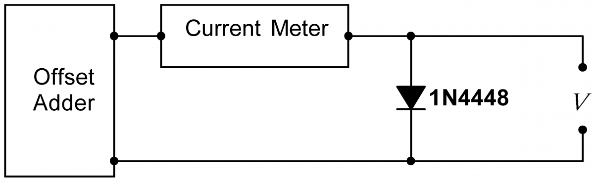
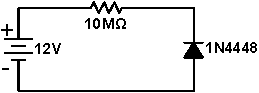
Problem 3.6 - Diode Reverse Current
|
Build the circuit at right. Measure the reverse diode current at approximately $-12\,\mathrm{V}$. The current is too small to measure directly, so use the Keithley 2110 DMM to measure the voltage across the resistor, and Ohm's law to infer the current. Remember that the Keithley has an input impedance of $10\,\mathrm{M}\Omega$; you will have to consider this impedance to properly calculate the reverse diode current. Compare your answer to the value of $-I_\mathrm{sat}$ that you found in problem 3.5. Junction imperfections in real diodes often cause the reverse biased current to be bigger than $-I_\mathrm{sat}$ However, Eq. (1), with the ideal value of $I_\mathrm{sat}$, is still valid in the forward region. |
 |
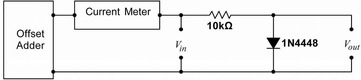
Problem 3.7 - Diode Equilibrium
|
Using the same diode as before, build the circuit shown at right. Vary $V_{in}$ by turning the Offset Adjust knob on the Offset Adder. What is the current $I$ and the voltage $V_{out}$ for $V_{in} = 0.5, 0.7,1,2,4,$ and $8\,\mathrm{V}$? Replace the $10\,\mathrm{k}\Omega$ resistor with a $1\,\mathrm{k}\Omega$ resistor. Again measure the current and output voltage for several input voltages. Using the graph of the diode characteristic you obtained in problem 3.5, perform a graphical load line analysis for each of the resistors. Do the equilibrium points predicted by the load line analysis agree with your data? |
 |
Problem 3.8 - Offset Adder Functionality II
Connect the signal generator to the input of the Offset Adder. Now, the output of the Offset adder will be the sum of the signal connected to the Offset Adder’s input, and the internal offset set by the Offset Adjust knob.
Examine the Offset Adder’s output on the scope, and play with different offsets and inputs until you understand the Offset Adder’s function.
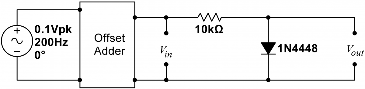
Problem 3.9 - Small-Signal Behavior
|
Build the circuit at right. Adjust the signal generator and Offset Adder to produce a $0.1\,\mathrm{Vpp}$ sine wave riding on a $+0.4, +0.6,$ and $0.8\,\mathrm{V}$ DC offset. Save images of the traces for $V_{in}$ and $V_{out}$ for each offset voltage. Also record the amplitude of the AC component of $V_{out}$ for each offset voltage; you will use these values later. |
 |
Since diodes carry current only in one direction, they can be used to rectify AC signals; rectify means to convert an AC signal into DC. Consequently, diodes are sometimes called rectifiers, especially when used in this application.
There are a few electronic circuits, like light dimmers and some electric motor controllers, that run off of AC. Most non-battery-powered electronics, however, require that the AC from a wall socket be converted to DC.
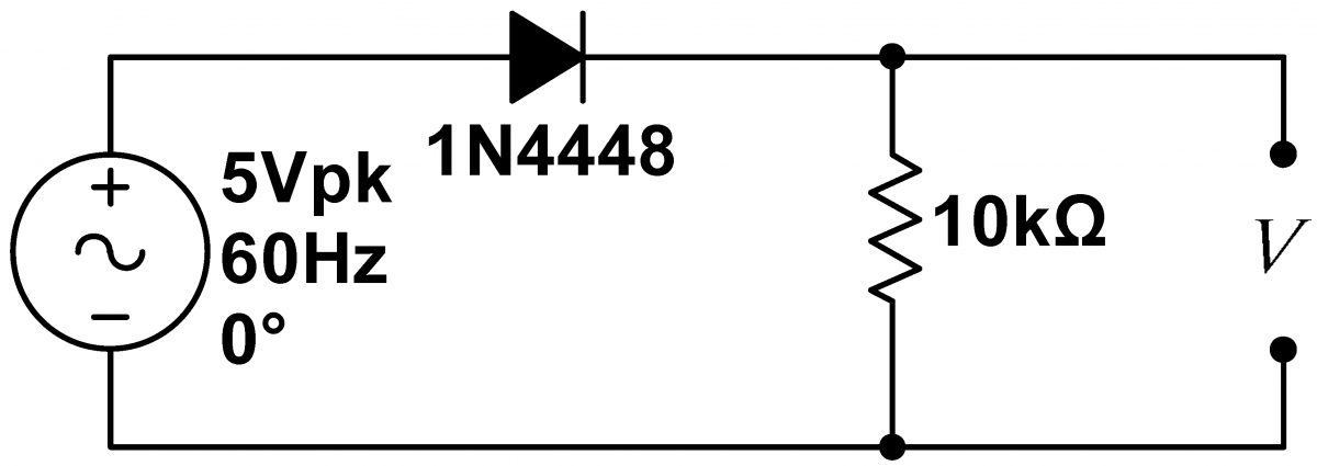
Problem 3.10 - Half Wave Rectification
|
Build the half-wave rectifier circuit at right. Use the signal generator to generate a $5\,\mathrm{Vpp}$, $60\,\mathrm{Hz}$ sine wave. Display the output of the signal generator on channel 1 of the scope, and the voltage across the resistor on channel 2. This latter voltage is the output of the circuit. Save images of the traces, and explain all the features of the output voltage. |
 |
|
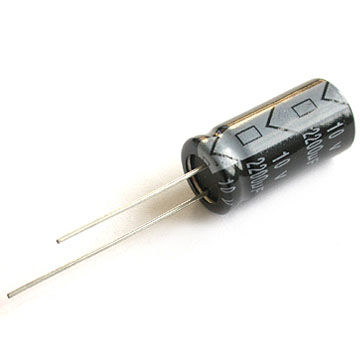
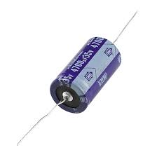
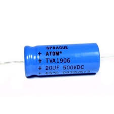
Rectification, as provided by the previous circuit, is only the first step in converting AC power into DC power. The gross irregularities in the signal produced by the above circuit needs to be smoothed out, typically by a high-capacitance filter capacitor. Because of technological limitations, the "ceramic" capacitors that you have been using up to now do not have sufficiently high capacitance to be used in this application. Consequently, the exercises below use electrolytic capacitors. Unlike ceramic capacitors, electrolytic capacitors are polarized. One lead of a polarized capacitor must be held at a negative potential relative to the other. The negative lead is typically marked with a stripe containing stylized minus signs or zeros, and sometimes with an arrow. Alternatively, axial capacitors are sometimes marked with a detent and plus signs on the positive lead. Three styles of electrolytic capacitors are shown at right. |
Radial Capacitor Negative lead on top |
Axial Capacitor I Negative lead at right |
Axial Capacitor II Positive lead at left |
|
What happens if you reverse bias a capacitor? They can explode...watch the video at right. Even if the capacitor doesn't explode, it will be damaged if it is ever reversed biased: its capacitance will go down, and its leakage resistance (a resistance through the capacitor that is infinite in an ideal capacitor, and nearly so in a ceramic capacitor) will diminish. In general, electrolytic capacitors will not perform as well as ceramic capacitors. Always use a ceramic capacitor if one is available in the required size. Electrolytic capacitors (and a slightly better performing type of capacitor called a tantalum capacitor) should only be used for applications like rectification filtering. Never use one for a normal high or low pass filter, and never use them in circuits in which they can ever be reverse biased. |
|||
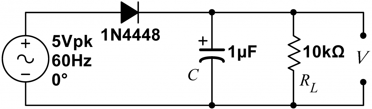
Problem 3.11 - Filtered Half Wave Rectification
|
Add a $10\,\mu\mathrm{F}$ capacitor to your circuit. (If you use an electrolytic capacitor, make sure you obey the polarity markings on the capacitor body.) Save images of the output waveform. Note the amplitude of the ripple. How does it change when you: a) Double the input frequency; b) Double the filter capacitor $C$; c) Double the load resistor $R_L$? (See analysis question 3.15) |
 |
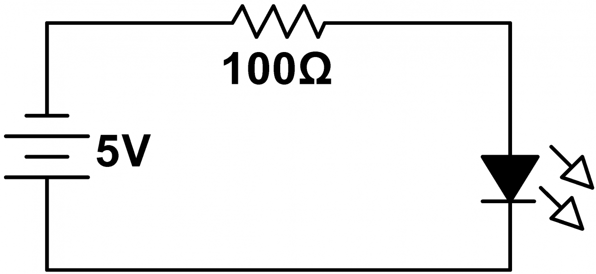
Problem 3.12 - Light Emitting Diodes (LEDs)
LEDs are diodes made from the semiconducting material Gallium Arsenide (GaAs) rather than from silicon. GaAs junctions have the very useful property that they emit light when forward biased.
|
Construct the circuit at right using a red LED for the diode. The LED should not light. Measure the voltage across the resistor to demonstrate that no current is flowing. Now swap the power supply polarity; the LED should now light. Measure the voltage drop across the resistor and LED. and calculate the current trhough the LED. Substitute 300$\Omega$, 3k$\Omega$, 30k$\Omega$, and 300k$\Omega$ resistors for the 100$\Omega$ resistor. How does the brightness of the LED change? How does the forward voltage drop change? How much current is required to light the LED? |
 |
Problem 3.13 - LED Characteristic Curves
Compare the characteristic curves of red, green, and blue LEDs. What fundamental constant partially explains your observations?
Problem 3.14 - Zener Diodes
Circuits frequently require DC voltages less than the circuit power supply voltage. Such voltages can be obtained with voltage dividers, but dividers are not stiff and, consequently, their output voltage will decrease when loaded. Furthermore, the divider voltage will follow any power supply voltage fluctuations.
Better schemes use a device called a Zener diode. Zener diodes are diodes deliberately optimized for use in the reverse breakdown region. Use the Curve Tracer to obtain the characteristic curve of a 1N5234B $6.2\,\mathrm{V}$ Zener diode. (Make sure you switch from the Diode Tracer window to the Zener Diode Tracer window.)
Using a Zener diode in the lower leg, you can make a voltage divider-like circuit whose ouput voltage is quite stiff, i.e. independent (up to a point) of the load, and largely independent of the input voltage. A resistor, $R_s$, should be used in the upper leg.
Design and build a circuit with the Zener that will reduce a voltage from 12V to 6.2V. The current going through $R_s$ should be limited to about $15\,\mathrm{mA}$. Hint: considering the Zener's characteristic curve, should the Zener be forward or reverse biased?
What is the smallest load resistor $R_\mathrm{L}$, a resitor placed in parallel with the diode, that will not significantly decrease the circuit output voltage? [The resistor $R_s$ is NOT the load resistor. Do not try small values for $R_s$]
Problem 3.15 - Frequency Doubling
Many nonlinear devices (including diodes) exhibit the very useful phenomenon of frequency doubling: when driven by a sufficiently high amplitude signal, they double the signal’s frequency. Frequency doubling is for instance, employed to produce short-wavelength coherent light. Few lasers laze in blue or shorter wavelengths. Powerful red lasers, however, are easy to build. The output from such red lasers can be fed into a frequency doubling crystal, and blue light will come out. This blue light can then be fed into another crystal, yielding ultraviolet light. Although the process is lossy, frequency doubling is the most effective way of making intense, short-wavelength laser pulses.
We will study frequency doubling in a Spice diode circuit. Run MultiSim, and load the Desktop\Mulitisim\Lab 3\BiasDiod schematic.
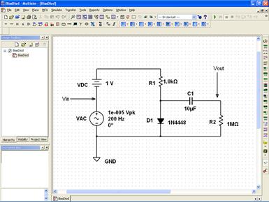
In this circuit, capacitor C1 is used to block the DC component of the signal across the diode. Measure the output of the circuit across R2, the load. VAC sets the amplitude of the AC signal driving the diode, while VDC (1V) sets the DC bias. Both VAC and VDC can be changed by double clicking on the numeric value to their right.
Set VAC to 0.00001. Here nonlinear effects are negligible. Run MultiSim, and look at the output by running an AC Analysis (Simulate →Analyses → Transient Analysis). The graphics program will pop up with a display of the input signal (at the amplitude 0.00001V) and the smaller output signal. As both waveforms look like perfect sine waves, it is difficult to determine the purity of the waves directly from these plots. The best way to determine their spectral content is to find their Fourier representation. Use Simulate→ Analyses→ Fourier Analysis The display will change to graphs of the Input and Output harmonic content. Both waves are nearly pure sine waves (note the log vertical scale.) There will be some high order harmonics, but their amplitude will be many orders of magnitude lower.
Now go back to the schematic and adjust VAC to 1V. Rerun the simulation, and note the gross distortion of the output wave. Look at the FFT display: there will now a whole series of slowly decreasing higher harmonics. The first few harmonics will not be that much lower in amplitude.
Play with VAC. What is the lowest amplitude input signal required for significant frequency doubling? (There is no hard threshold.) Are the harmonics ever stronger than the fundamental? Why do you think the frequency doubling occurs?
The remaining problems can be done away from the lab.
Problem 3.16 - Rectifier Ripple
Find an (approximate) expression for the (peak-to-peak) amplitude of the ripple in the rectifier built in 3.11 as a function of the input voltage and frequency, load resistor, and filter capacitor. Does your model agree with your observations?
Problem 3.17 - Small Signal Analysis I
Find the operating point for the circuit in 3.9 for all three offset voltages. Then perform a graphical perturbation analysis for the three offsets to predict the AC component of $V_{out}$. Use the diode characteristic curve you obtained in 3.5.
Problem 3.18 - Small Signal Analysis II
Now repeat 3.17 using the small signal impedance perturbation technique: calculate the small signal impedance of the diode at each operating point; then use this impedance in a “linear” voltage divider analysis. Show how the large-signal impedance would yield a voltage divider output much greater than the actual answer.
Please fill out the